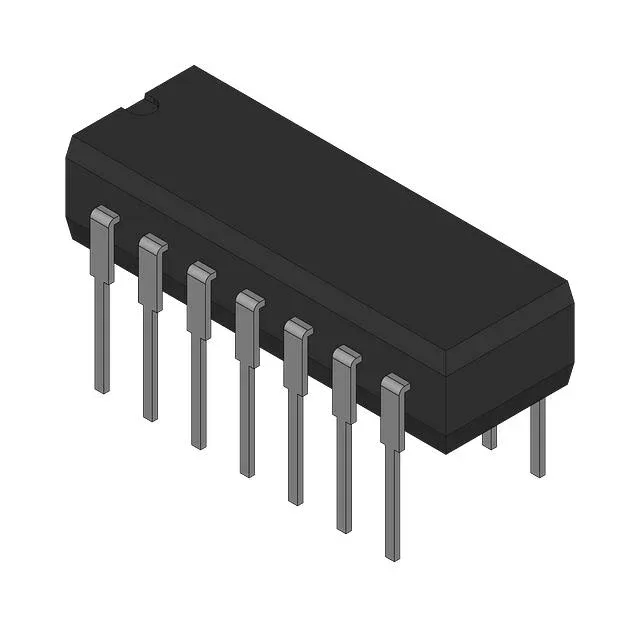
Quad JFET op-amp in a hermetic 14-CDIP
The 8102306CA is a quad JFET-input operational amplifier in a 14-lead ceramic DIP (14-CDIP) package.
At 13 V/µs, the output can swing 10 V in under 800 ns, which is enough to reproduce a 100 kHz sine wave cleanly at full output. The 3 MHz GBW product means the gain-bandwidth trade-off is typical for a general-purpose JFET op-amp: you can set a gain of 10 and still have a 300 kHz closed-loop bandwidth. If your application needs to track fast transients — say, a current-sense amplifier in a motor drive — the slew rate is the number that keeps the output from slewing into distortion.
JFET input: low bias, high impedance
The 65 pA input bias current is the hallmark of a JFET front end. It lets you use high-value feedback resistors (1 MΩ and up) without the offset voltage drifting with temperature the way a bipolar input would. For photodiode amplifiers, pH probe buffers, or any circuit where the source impedance is in the megaohm range, the JFET input is the right choice.
Package and temperature: built for the harsh stuff
The 14-CDIP (0.300" body, 7.62 mm width) is a through-hole ceramic package with a hermetic seal. It is the standard for military and aerospace programs that specify MIL-STD-883 screening. The through-hole mounting means it can be socketed — a real advantage for field-service swaps without a hot-air station.
Supply range and quiescent current
The 10 V to 30 V supply span gives you headroom for ±5 V to ±15 V split rails or a single 12 V or 24 V industrial rail. Total quiescent current for all four amplifiers is 1.4 mA (350 µA per channel), which is modest for a quad JFET part — it keeps the self-heating low in the ceramic package, where thermal resistance is higher than in plastic.