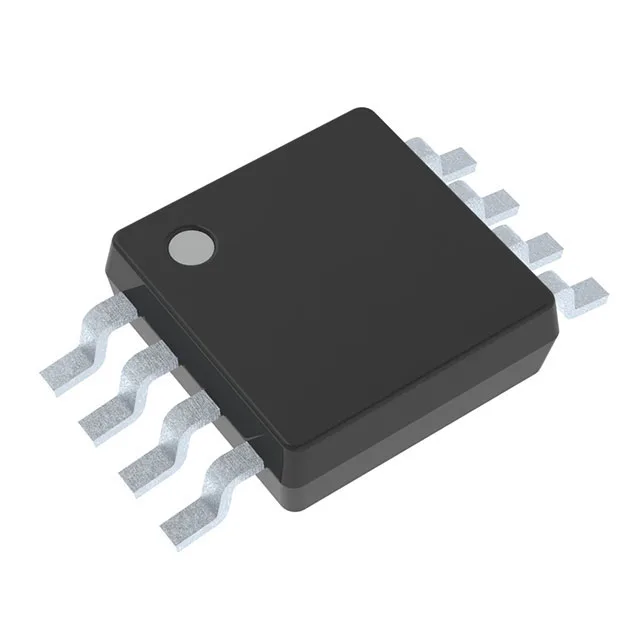
Each of the two elements handles one bit, giving you two independent buffer channels in a single 8-pin VFSOP or VSSOP package. The 3-state outputs let you connect multiple buffers to a shared bus — when the output enable is inactive, the output goes high-impedance instead of fighting the bus. With a supply range from 1.65V to 5.5V, this part bridges 1.8V, 2.5V, 3.3V, and 5V logic domains without a level shifter.
If you have this part on a legacy BOM, you are looking at the surplus and broker channel for any remaining stock. The good news is that the 74LVC2G241 function is widely second-sourced — the SN74LVC2G241 from TI (different package suffix) and equivalents from NXP, ON Semiconductor, and others are pin-compatible and electrically identical. For new designs, skip this obsolete suffix and specify the active SN74LVC2G241 variant in the package you need.
Output drive and supply — sizing the rail
That drive strength lets you directly light a standard LED, drive the base of a small-signal transistor, or fan out to several CMOS inputs without a separate buffer stage. The 1.65V minimum supply means this part works with a single Li-ion cell (3.0V-4.2V) all the way down to near-depleted (1.65V), so it is a natural fit for battery-powered portable equipment. The 5.5V maximum covers 5V TTL logic rails cleanly, with 5V-tolerant inputs that do not draw excessive current when driven above VCC.
Package and footprint — what you are soldering
The DCUTE4 suffix indicates a Tape & Reel shipping format, but the device itself is housed in an 8-VFSOP package (2.30mm width, 0.091" body length) or the functionally identical 8-VSSOP. Both are fine-pitch surface-mount packages — about 2.3mm wide, so they fit in tight board layouts. The small body means the thermal mass is low; standard reflow profiles for lead-free solder work fine.