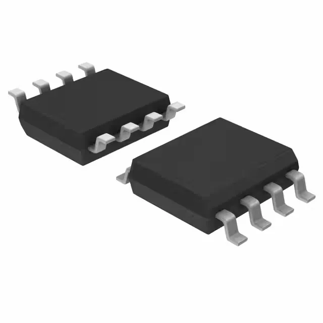
Dual buffer with 3-state outputs for mixed-voltage buses
The 74LVC2G241DCTRG4: Each of the two elements drives up to 32 mA per channel, sufficient for buffering address/data lines or driving LED indicators directly. The 3-state output control allows multiple devices to share a common bus without contention — a standard requirement for memory interfaces, peripheral buses, and I/O expansion.
At 1.65 V it still meets the 32 mA output drive, though the output voltage swing scales with VCC. For designs that must tolerate a 5 V bus while the core logic runs at 3.3 V, the 5.5 V absolute maximum on the supply pin (not stated here, but implied by the 5.5 V operating limit) provides the necessary overvoltage tolerance. The 74LVC family's 5 V tolerant inputs are a well-known feature — this part inherits that characteristic.
The 125°C upper limit covers under-hood automotive applications (though AEC-Q qualification is not cited in the ledger). For designs that only need 85°C, the margin is still useful for derating in high-power enclosures.
SM8 package — 8-lead MSOP with 2.80 mm body width
Housed in an 8-pin SM8 (MSOP-8) package with a 2.80 mm body width, the 74LVC2G241DCTRG4 occupies minimal board area. The surface-mount footprint is compatible with standard MSOP-8 land patterns. For hand-prototyping, the same die is available in other package options under the base number 74LVC2G241.
The base number 74LVC2G241 covers multiple package and tape options, so if the SM8 reel variant is temporarily constrained, a different package suffix (e.g., DCTR without the G4) may be cross-shopped — but verify pin compatibility first.