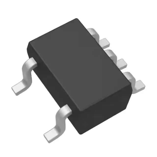
It operates across a wide supply range of 1.65V to 5.5V, making it usable with 1.8V, 2.5V, 3.3V, and 5V logic domains without a level translator. The 3-state output (high-Z when the output-enable pin is asserted) lets you connect it to a shared data bus or multiplexed signal line without contention.
Supply range and drive — the practical limits
The 1.65V to 5.5V supply means this buffer works with nearly any digital logic family in common use today: 1.8V FPGAs, 2.5V ASICs, 3.3V microcontrollers, and legacy 5V TTL/CMOS systems. The 32mA output drive is symmetric for high and low states, so you get equal fanout for both logic levels. At 5.5V the output impedance is lower, giving faster edge rates; at 1.65V the drive is still sufficient for a single CMOS load but the rise time increases — account for that in timing budgets at low supply.
Housed in a 5-pin SC-70 (SOT-353) package, the 74LVC1G125DCKRG4 occupies roughly 2.0mm × 2.1mm of board area. The small size suits dense mixed-signal boards where a single buffer is needed to clean up a clock signal or isolate a control line — no need to route to a larger SOIC or TSSOP package.