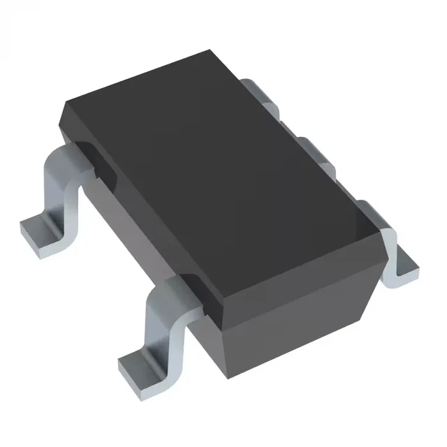
Single-gate buffer for bus isolation and level translation
The output can sink or source 32 mA, enough to drive a logic-level LED or a short cable stub without an external transistor.
At the low end, 1.65 V is below the typical 1.8 V rail, so the part stays operational during brownout or cold-crank conditions. No derating needed for the full range — the 125°C ceiling is the junction limit, not a derated figure.
Output drive and 3-state control
The ±32 mA output drive is symmetric — the high and low current ratings are identical at 32 mA each. That means the buffer can drive a bus line with equal rise and fall times, which simplifies timing closure on a shared data line. The 3-state output (high-impedance when the output-enable pin is inactive) lets multiple buffers share a common bus without contention. For a single-gate part, the drive is generous — enough to sink a standard LED directly (with a series resistor) or to drive the input of a high-impedance ADC without a buffer stage.
That means no last-time-buy scramble, no broker premium for old-date-code stock. For BOM planning, this is a low-risk line item: single-sourced from TI, but the 74LVC family is widely second-sourced by other manufacturers with pin-compatible parts (e.g., NXP, ON Semiconductor). If you need a drop-in alternate for dual-sourcing, look for a 74LVC1G125 in the same SOT-23-5 footprint from any of those vendors — the logic function and pinout are industry-standard.