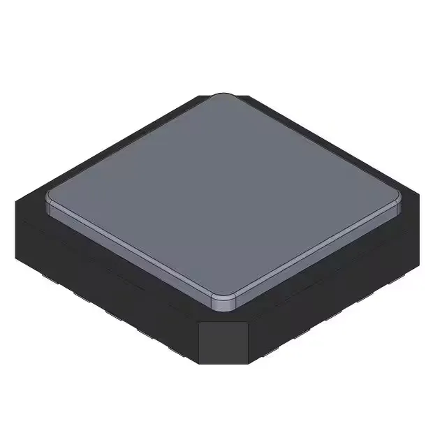
Dual JFET op-amp in a hermetic 20-CLCC for harsh environments
The 5962-9460202Q2A is a dual JFET-input operational amplifier from a standard military/aerospace product line, packaged in a 20-CLCC ceramic leadless chip carrier. Each of the two channels can source or sink 48 mA. This part is designed for signal conditioning in avionics, satellite, downhole instrumentation, and other sealed or high-reliability systems where the hermetic package prevents moisture ingress and the wide temperature range guarantees operation outside the commercial envelope.
The 40 V/µs slew rate and 10 MHz gain-bandwidth product support fast pulse and high-frequency analog signals. The 20 pA input bias current suits high-impedance sources.
Hermetic 20-CLCC — why the package matters
The 20-CLCC (ceramic leadless chip carrier) is a hermetic, surface-mount package measuring 8.89 mm square. Unlike plastic SOIC or TSSOP, the ceramic body and sealed lid prevent moisture and contaminant ingress, which is critical for long-life missions, vacuum environments, or high-humidity industrial settings. The surface-mount footprint matches standard LCCC land patterns, but the thermal expansion coefficient of the ceramic substrate must be considered when soldering to FR4 — a controlled-profile reflow with a slow ramp rate reduces mechanical stress on the solder joints.