Output drive and 3-state bus control
The 5962-9221303MRA: 12mA source and 48mA sink per output — the asymmetric drive is typical of bipolar TTL-compatible logic, where the low-level (sink) current handles the heavier load of a bus termination or LED driver. The 3-state output lets you disable each element's outputs into high-impedance — multiple buffers can share a data bus without contention, and the OE control ties directly to a microcontroller GPIO or address decoder. With two elements per package, you get eight inverting channels in one DIP — useful for signal inversion banks, address-line buffering, or parity generation where board space is tight.
Military-grade temperature and ceramic package
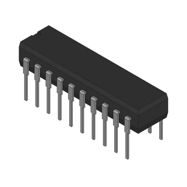
The ceramic DIP handles the thermal expansion mismatch of PCB materials across the range without solder-joint fatigue. The 20-CDIP package has a 0.300-inch body width — standard DIP footprint, 0.100-inch pin pitch. Through-hole mounting means it survives higher vibration and thermal cycling than a surface-mount SOIC of the same pin count. Supply voltage tolerance of 4.5V to 5.5V covers the full 5V ±10% rail — no external regulator needed if the board's 5V bus is within that window.