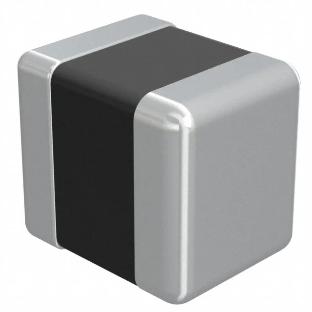
The LBC2016T2R2MV: This status means the part remains available for existing production BOMs but is not intended for new design-ins. For a procurement decision, this flags a limited procurement window — the manufacturer may issue a last-time-buy notice without extended lead time.
2.2 µH at 520 mA — the DC bias operating point
The LBC2016T2R2MV is a wirewound inductor rated 2.2 µH at a test frequency of 7.96 MHz, with a ±20 % tolerance. The 520 mA current rating is the DC bias current at which the inductance typically drops by 10 % — above this current the inductance rolls off faster. For a power rail filter or DC-DC converter output choke, the peak load current should stay below 520 mA to maintain the nominal inductance value. DC resistance is 200 mOhm, which sets the I²R conduction loss at 54 mW at full rated current. In a 105°C ambient, this self-heating adds to the thermal budget — the 0806 package dissipates this without exceeding the rated temperature when the board copper area follows the standard footprint.
AEC-Q200 qualification and deployment envelope
Unshielded construction means the magnetic field radiates from the winding — adjacent traces carrying sensitive analog signals or high-speed digital lines should maintain a keep-out zone of at least twice the component height (3.6 mm) to avoid coupling. For EMI-sensitive designs, a shielded inductor in the same footprint is the alternative.
0806 footprint and board integration
This is a standard two-pad footprint — the solder pad dimensions per the IPC-7351B nominal land pattern are 1.00 mm x 1.20 mm per pad with a 2.20 mm pad-to-pad centre distance. The 1.80 mm height clears most low-profile enclosures and allows placement under a 2.0 mm board-to-cover gap. Surface-mount assembly on standard FR-4 with a 0.10 mm solder paste stencil aperture per pad gives a self-alignment margin of ±0.15 mm during reflow. The component is supplied on tape and reel (embossed carrier, 8 mm tape width) for automated pick-and-place at up to 15,000 components per hour.