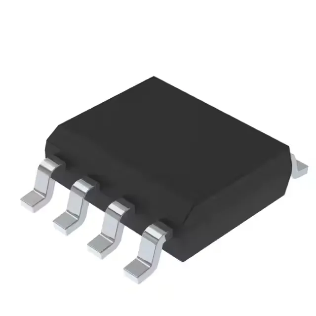
STMicroelectronics TS512IYDT — Logic ICs

STMicro TS512IYDT General Purpose Op-Amp, 3 MHz, AEC-Q100

MPNTS512IYDT
End of Life

STMicroelectronics TS512IYDT, dual general-purpose op-amp, 3 MHz gain bandwidth, 1.5 V/µs slew rate, 500 µA per channel supply, -40 to 125 °C, AEC-Q100, 8-SOIC package.

$3.41Ref. price · indicative, final on quote
Packaging8-SOIC (0.154", 3.90mm Width)
StockContact for availability
MOQ1 pcs
  • 100% new & originalTraceable channels only — no refurbs, no pulls, no remarked parts.
  • Date & lot codes on quoteStated per line before you commit; label photos on request.
  • MSL-compliant ESD packingMoisture-sealed bags with indicator cards; reels photo-verified.
  • PayPal buyer protectionPay by T/T, PayPal or Payoneer — card payments covered end to end.

Specifications

TS512IYDT Technical Specifications
ParameterValue
SeriesAutomotive, AEC-Q100
Mounting typeSurface Mount
Amplifier typeGeneral Purpose
Voltage - input offset500 µV
Voltage - supply span30 V
Current - supply500µA (x2 Channels)
Current - input bias50 nA
Current - output (Channel)23 mA
Operating temperature-40°C ~ 125°C
Gain bandwidth product3 MHz
PackageTape & Reel (TR); Cut Tape (CT)
Slew rate1.5V/µs
Case8-SOIC (0.154\", 3.90mm Width)
Number of circuits2

Product details

3 MHz GBW at 500 µA — balancing speed against quiescent draw

At 3 MHz gain-bandwidth the TS512IYDT sits a step faster than the 1.4 MHz TSV358IDT and TSV358AIDT siblings, which matters when conditioning signals from a resolver or a shunt-based current sensor where the loop needs to settle inside a few microseconds. The 1.5 V/µs slew rate keeps large-signal distortion low on a 5 V or 12 V rail. Meanwhile the 500 µA per-channel supply is roughly half what a 4 MHz TS924IYPT draws, so the TS512IYDT is the pick for always-on automotive modules where every milliamp counts.

Supply range and offset — what they mean for a 12 V automotive rail

The TS512IYDT runs from a 3 V to 30 V supply span, so it handles a 12 V battery rail with margin through cold-crank and load-dump transients (within the 30 V max). Input offset voltage is specified at 500 µV maximum, which is typical for a general-purpose amplifier and adequate for most sensor conditioning roles — if sub-100 µV offset is needed, the TSV358AIDT with its 100 µV max is a better fit. Input bias current is 50 nA, low enough that it doesn't dominate error in a 10 kΩ divider.

Package and mounting

The surface-mount package is MSL 1 typically, so no bake required before assembly as long as the reel hasn't been soaked in a humid environment. The low pin count and wide lead pitch mean hand rework is straightforward; just pre-tin the pads, align by the chamfer, and touch each lead with the iron.

RoHS3 compliant per the listing. The AEC-Q100 qualification is documented, which satisfies the PPAP requirements for most Tier-1 automotive programs.

Frequently asked questions

Will TS512IYDT drop into a panel that was specified around TSV358IDT without rewiring?

The TS512IYDT is pin-compatible in the same 8-SOIC package, so the PCB footprint is identical. However, the TS512IYDT has a 3 MHz GBW versus 1.4 MHz on the TSV358IDT, and the input offset is 500 µV max versus 200 µV on the TSV358IDT. If the original design relied on the TSV358's lower offset or its rail-to-rail output, verify those margins before swapping — the TS512IYDT output is not rail-to-rail.