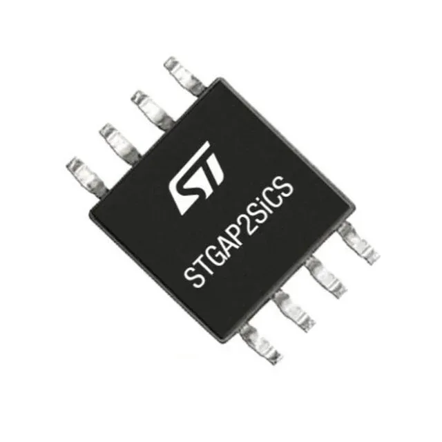
STMicroelectronics STGAP2SICSC — Power Management (PMIC / Gate Driver)

STGAP2SICSC Gate Driver, 4A, 5000Vrms, 8-SOIC

MPNSTGAP2SICSC
End of Life

STMicroelectronics STGAP2SICSC isolated single-channel gate driver, capacitive coupling, 5000Vrms, 4A peak output, 30ns typ rise/fall, 100V/ns min CMTI, -40 to 125°C, 8-SOIC (7.50mm width), Tube.

$2.89Ref. price · indicative, final on quote
Packaging8-SOIC (0.295", 7.50mm Width)
RoHSROHS3 Compliant
Independent supplier — new & surplus stockAuthenticity-screened · ESD-safe packingListing updated Aug 2026

Specifications

STGAP2SICSC specifications
ParameterValue
MountingSurface Mount
Voltage - isolation5000Vrms
Voltage - output supply3V ~ 5.5V
Current - peak output4A
Current - output high, low4A, 4A
Operating temperature-40°C ~ 125°C
Pulse width distortion20ns
Approval agencyUL
PackageTube
TechnologyCapacitive Coupling
Case8-SOIC (0.295\", 7.50mm Width)
Channels1
Rise (Fall time)30ns, 30ns
Propagation delay tpLH (tpHL)90ns, 90ns
Common mode transient immunity100V/ns

Product details

Single-channel isolated gate driver for SiC and IGBT switching stages

The STMicroelectronics STGAP2SICSC is a single-channel isolated gate driver built around capacitive coupling technology, delivering 4 A peak output current with 30 ns typical rise and fall times. It is designed to drive SiC MOSFETs, IGBTs, and power MOSFETs in medium-to-high-voltage switching stages where galvanic isolation between the controller and the power device is required. The 5000 Vrms isolation rating and 100 V/ns minimum common-mode transient immunity (CMTI) suit it for motor drives, industrial power supplies, solar inverters, and automotive traction inverters where fast switching edges and noisy environments are the norm. The part is rated over -40 °C to 125 °C, covering the thermal extremes inside a sealed power converter or under-hood electronics bay.

Supply and logic interface

The output-side supply range is 3 V to 5.5 V. Propagation delay is 90 ns maximum in both directions, with pulse-width distortion held to 20 ns maximum.

Frequently asked questions

What is the pinout of the STGAP2SICSC?

The STGAP2SICSC is supplied in an 8-SOIC wide-body package (7.50 mm width). The pinout follows the standard isolated gate driver pin arrangement for this footprint; consult the STMicroelectronics datasheet for the exact pin assignments.

Is STGAP2SICSC compatible with 3.3V logic?

Yes. The output supply range is 3 V to 5.5 V, so the driver accepts both 3.3 V and 5 V logic inputs directly without external level translation.

What is the maximum operating temperature for STGAP2SICSC?

The operating temperature range is -40 °C to 125 °C, covering industrial and automotive under-hood environments.

What is the closest pin-compatible alternative to STGAP2SICSC?

Within the STGAP2 family, the STGAP2SICS (non-C variant) and STGAP2SICSTR (tape-and-reel variant) share the same 8-SOIC footprint and functional ratings. The 'C' suffix indicates capacitive coupling technology; the non-C variant uses a different isolation technology. Verify the isolation rating and CMTI for your specific application before substituting.