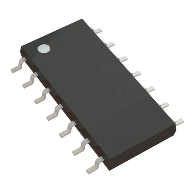
Quad JFET op-amp for multi-channel analog signal conditioning
The STMicroelectronics TL064CDT is a quad JFET-input operational amplifier in a 14-SOIC package, combining four independent op-amps on one die. Its JFET input stage delivers 30 pA typical input bias current, making it suitable for high-impedance sensor interfaces, photodiode amplifiers, and precision integrators where bipolar input stages would load the source. Each of the four channels draws 200 µA supply current, keeping the total package dissipation under 1 mA quiescent — a meaningful advantage for multi-channel data acquisition or signal conditioning on a shared power rail.
The 6 V to 36 V supply span covers single-supply 5 V, 12 V, and 24 V industrial rails, as well as split supplies from ±3 V to ±18 V. This flexibility lets the same BOM line serve different rail voltages across a product family without requalifying the op-amp.
Slew rate and bandwidth — what the 3.5 V/µs and 1 MHz mean for signal fidelity
For a 1 V peak-to-peak output swing, the full-power bandwidth is roughly 550 kHz — adequate for audio-frequency processing, low-speed ADC drivers (e.g., 10 kSPS to 100 kSPS SAR converters), and active filter stages below 100 kHz. The 20 mA per-channel output current drives typical feedback networks, reference buffers, and moderate cable loads, but is not intended for high-current line drivers or headphone amplifiers. The 3 mV input offset voltage is a typical value; for precision DC applications requiring sub-millivolt offset, a chopper-stabilized or auto-zero amplifier would be a better fit.
Package and footprint — 14-SOIC surface-mount assembly
It is a surface-mount device intended for reflow soldering on standard FR-4 PCBs. The supplier device package is 14-SO.
The ROHS3 compliance covers the current regulatory requirements for lead-free assembly.