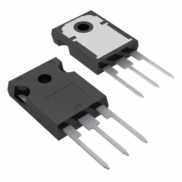
STMicroelectronics STW72N60DM2AG

STW72N60DM2AG N-Channel MOSFET, 600 V, 66 A, TO-247-3

MPNSTW72N60DM2AG
End of Life

STMicroelectronics STW72N60DM2AG, Automotive AEC-Q101 MDmesh DM2 N-Channel MOSFET, 600 V Vdss, 66 A Id, 42 mOhm Rds(on) at 10 V, TO-247-3 through-hole package.

$12.04Ref. price · indicative, final on quote
PackagingTO-247-3
StockContact for availability
MOQ1 pcs
  • 100% new & originalTraceable channels only — no refurbs, no pulls, no remarked parts.
  • Date & lot codes on quoteStated per line before you commit; label photos on request.
  • MSL-compliant ESD packingMoisture-sealed bags with indicator cards; reels photo-verified.
  • PayPal buyer protectionPay by T/T, PayPal or Payoneer — card payments covered end to end.

Specifications

STW72N60DM2AG Technical Specifications
ParameterValue
SeriesAutomotive, AEC-Q101, MDmesh™ DM2
FET typeN-Channel
Mounting typeThrough Hole
Drain to source voltage600 V
Drive voltage (Max rds on, min rds on)10V
Current - continuous drain (Id) @ 25°C66A (Tc)
Power dissipation446W (Tc)
Operating temperature-55°C ~ 150°C (TJ)
PackageTube
Vgs±25V
TechnologyMOSFET (Metal Oxide)
CaseTO-247-3
Vgs(th) (Max) @ id5V @ 250µA
Rds on (Max) @ id, vgs42mOhm @ 33A, 10V
Gate charge (Qg) (Max) @ vgs121 nC @ 10 V
Input capacitance (Ciss) (Max) @ vds5508 pF @ 100 V

Product details

600 V, 66 A N-channel MOSFET for automotive power trains

It is qualified to AEC-Q101, making it suitable for automotive power conversion and motor drive applications where reliability under thermal and electrical stress is required.

On-resistance and gate charge — conduction and switching losses

This Rds(on) figure sets the conduction loss floor at a given current; at 33 A the dissipation is roughly 46 W (I²R), which must be managed within the 446 W maximum power dissipation rating. Total gate charge is 121 nC at 10 V. For a 20 kHz switching frequency, the average gate-drive current required is about 2.4 mA; the driver must supply this without exceeding its peak current capability during the switching transition. Input capacitance Ciss is 5508 pF at 100 V drain-source. This capacitance, together with the gate resistance, sets the switching speed and the Miller plateau duration; a higher Ciss slows the turn-on and turn-off edges, increasing crossover losses if the gate drive is not sized accordingly.

Temperature range and package — mounting and thermal management

Operating junction temperature range is -55 °C to 150 °C, covering automotive under-hood and chassis environments. The TO-247-3 through-hole package provides a large copper tab for heatsinking; the thermal pad area on the PCB or heatsink must be sized to keep the junction below 150 °C at the maximum load current.

It is ROHS3 compliant, meeting the latest European restriction-of-hazardous-substances directive.

Frequently asked questions

What is the exact Rds(on) of STW72N60DM2AG at 10V Vgs?

The maximum on-resistance is 42 mOhm at a drain current of 33 A with a 10 V gate-to-source drive. This is the worst-case figure at 25 °C junction temperature; actual Rds(on) increases with temperature per the normalised curve in the datasheet.

Can STW72N60DM2AG replace STW70N60DM2?

The STW72N60DM2AG is a higher-current variant in the same MDmesh DM2 family, with a 66 A continuous drain rating versus the STW70N60DM2's lower current. Both share the TO-247-3 package and 600 V Vdss, but the gate charge and Rds(on) differ. Verify the gate-drive and thermal budget against the original design before substituting.

What is the maximum junction temperature for STW72N60DM2AG?

The maximum operating junction temperature is 150 °C.