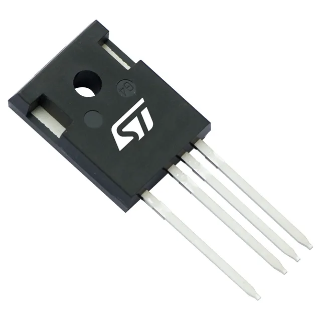
STMicroelectronics STW68N65DM6-4AG

STW68N65DM6-4AG MOSFET N-CH 650V 72A TO247-4, AEC-Q101

MPNSTW68N65DM6-4AG
End of Life

STMicroelectronics MDmesh™, N-Channel MOSFET, 650 V, 72 A, 39 mOhm Rds(on), 118 nC Qg, TO-247-4, AEC-Q101, -55 to 150 °C.

$11.84Ref. price · indicative, final on quote
PackagingTO-247-4
StockContact for availability
MOQ1 pcs
  • 100% new & originalTraceable channels only — no refurbs, no pulls, no remarked parts.
  • Date & lot codes on quoteStated per line before you commit; label photos on request.
  • MSL-compliant ESD packingMoisture-sealed bags with indicator cards; reels photo-verified.
  • PayPal buyer protectionPay by T/T, PayPal or Payoneer — card payments covered end to end.

Specifications

STW68N65DM6-4AG Technical Specifications
ParameterValue
SeriesMDmesh™
FET typeN-Channel
Mounting typeThrough Hole
Drain to source voltage650 V
Current - continuous drain (Id) @ 25°C72A (Tc)
Power dissipation480W (Tc)
Operating temperature-55°C ~ 150°C (TJ)
GradeAutomotive
PackageTube
Vgs±25V
TechnologyMOSFET (Metal Oxide)
QualificationAEC-Q101
CaseTO-247-4
Vgs(th) (Max) @ id4.75V @ 250µA
Rds on (Max) @ id, vgs39mOhm @ 36A, 10V
Gate charge (Qg) (Max) @ vgs118 nC @ 10 V
Input capacitance (Ciss) (Max) @ vds5900 pF @ 100 V

Product details

650 V N-channel MOSFET for automotive traction and DC-DC stages

The STW68N65DM6-4AG: AEC-Q101 qualified for automotive applications.

Gate charge and switching loss budget

Total gate charge is 118 nC at 10 V gate drive. Input capacitance Ciss is 5900 pF at 100 V drain-source bias. This value, together with the gate resistance in the drive loop, determines the turn-on and turn-off delay — relevant for dead-time tuning in half-bridge topologies.

Package and thermal design

The TO-247-4 package adds a Kelvin-source pin (the fourth pin) that separates the gate-drive return from the power current path, reducing the voltage drop in the gate loop caused by source inductance. This lowers the risk of gate ringing at high di/dt. Maximum power dissipation is 480 W at the case, but the practical dissipation is set by the junction-to-case thermal resistance and the heatsink's ability to pull heat away. The operating junction temperature range is -55 °C to 150 °C.

Frequently asked questions

What is the difference between STW68N65DM6-4AG and STW68N65DM6?

The -4AG suffix indicates the TO-247-4 package with a Kelvin-source pin (four leads) and AEC-Q101 automotive qualification. The base STW68N65DM6 uses the standard three-pin TO-247 package and lacks the automotive-grade screening. Electrically the die is the same MDmesh™ generation, but the pinout differs — the fourth pin is the source Kelvin connection, not a drain or gate.