800 V N-channel in a TO-251 — where it fits
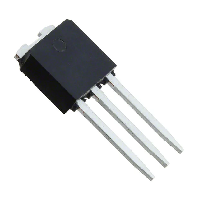
It comes in a TO-251-3 (IPAK) through-hole package — a compact three-lead footprint that suits high-density PCB layouts where a TO-220 would be overkill.
Conduction and switching — the numbers that matter
That 10 V drive requirement is standard for a high-voltage MOSFET; a 12 V gate-drive supply from a bias winding or bootstrap circuit covers it cleanly. Total gate charge is 16.5 nC at Vgs = 10 V. For a 100 kHz flyback converter, the gate-drive current needed is about 1.65 mA average — easily within the capability of a small driver IC. Input capacitance Ciss is 450 pF at Vds = 100 V, which keeps the Miller plateau short and limits switching losses.
Thermal and voltage headroom
Gate-source voltage is rated ±30 V, giving margin for ringing on the gate node in a hard-switching topology. The 800 V drain-source breakdown leaves headroom for 400 VDC bus rails in single-phase PFC or flyback stages with a 20% derating margin.