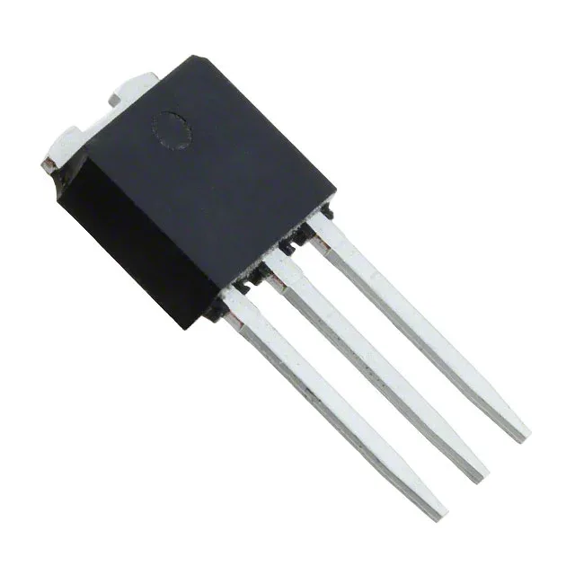
STMicroelectronics STU5N62K3

STU5N62K3 N-Channel MOSFET, 620V 4.2A, 1.6 Ohm Rds(on), IPAK

MPNSTU5N62K3
End of Life

STMicroelectronics SuperMESH3™ STU5N62K3, N-channel 620V 4.2A MOSFET, 1.6 Ohm Rds(on) at 10V, 26 nC gate charge, TO-251 (IPAK) through-hole, -55 to 150°C.

$1.77Ref. price · indicative, final on quote
PackagingTO-251-3 Short Leads, IPak, TO-251AA
StockContact for availability
MOQ1 pcs
  • 100% new & originalTraceable channels only — no refurbs, no pulls, no remarked parts.
  • Date & lot codes on quoteStated per line before you commit; label photos on request.
  • MSL-compliant ESD packingMoisture-sealed bags with indicator cards; reels photo-verified.
  • PayPal buyer protectionPay by T/T, PayPal or Payoneer — card payments covered end to end.

Specifications

STU5N62K3 Technical Specifications
ParameterValue
SeriesSuperMESH3™
FET typeN-Channel
Mounting typeThrough Hole
Drain to source voltage620 V
Drive voltage (Max rds on, min rds on)10V
Current - continuous drain (Id) @ 25°C4.2A (Tc)
Power dissipation70W (Tc)
Operating temperature-55°C ~ 150°C (TJ)
PackageTube
Vgs±30V
TechnologyMOSFET (Metal Oxide)
CaseTO-251-3 Short Leads, IPak, TO-251AA
Vgs(th) (Max) @ id4.5V @ 50µA
Rds on (Max) @ id, vgs1.6Ohm @ 2.1A, 10V
Gate charge (Qg) (Max) @ vgs26 nC @ 10 V
Input capacitance (Ciss) (Max) @ vds680 pF @ 50 V

Product details

620 V primary-side switch for offline flyback converters

Gate charge is 26 nC typ at 10 V drive, which keeps the switching loss manageable in a 50-100 kHz flyback primary without a high-current gate driver. The 680 pF input capacitance at 50 V drain-source confirms a modest drive requirement — a standard PWM controller output stage can drive it directly.

Package and board integration — TO-251 (IPAK)

The STU5N62K3 comes in a TO-251 (IPAK) through-hole package — three short leads, no tab screw hole, smaller than a full TO-220. The drain tab is the centre lead and is electrically live at the drain potential; the PCB layout must keep creepage clearance from the tab to low-voltage nodes. The package footprint matches the standard IPAK land pattern, with the tab soldered to a copper pad on the board for heat sinking. The 70 W power dissipation rating at case temperature assumes the tab is held at 25 °C — real-world derating follows the thermal resistance from junction to ambient, which depends on the PCB copper area under the tab.

Frequently asked questions

Is STU5N62K3 a suitable replacement for STP5NK60Z?

Both are 600 V-class N-channel MOSFETs from STMicroelectronics, but the STU5N62K3 has a 620 V drain-source rating versus 600 V for the STP5NK60Z. The STU5N62K3 carries 1.6 Ohm Rds(on) at 10 V gate drive, compared to 1.5 Ohm for the STP5NK60Z — a 6% difference that is negligible in most designs. The STP5NK60Z is in a TO-220 package; the STU5N62K3 is in a TO-251 (IPAK) through-hole package with a different footprint and tab geometry. Verify the PCB land pattern and heatsinking before substituting.

What is the gate charge and Rds(on) of STU5N62K3?

Gate charge (Qg) is 26 nC maximum at 10 V gate drive. On-resistance (Rds(on)) is 1.6 Ohm maximum at 2.1 A drain current and 10 V gate-source voltage.

What package does STU5N62K3 come in?

The STU5N62K3 is supplied in a TO-251-3 short-leads IPak package, also designated as TO-251AA. The supplier device package is TO-251 (IPAK). It is a through-hole package with three leads and a drain tab.