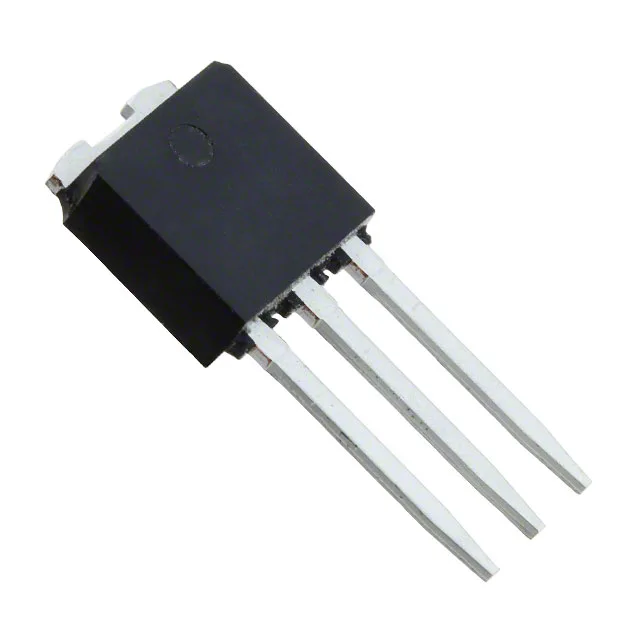
STMicroelectronics STU5N60M2

STU5N60M2 MOSFET N-Ch 600V 3.7A I-PAK, MDmesh II Plus

MPNSTU5N60M2
End of Life

STMicroelectronics MDmesh™ II Plus STU5N60M2, N-Channel MOSFET, 600 V Vdss, 3.7 A Id, 1.4 Ohm Rds(on) at 10 V, 4.5 nC Qg, I-PAK (TO-251) through-hole package, 150 °C junction temperature.

$1.43Ref. price · indicative, final on quote
PackagingTO-251-3, IPak, Short Leads
StockContact for availability
MOQ1 pcs
  • 100% new & originalTraceable channels only — no refurbs, no pulls, no remarked parts.
  • Date & lot codes on quoteStated per line before you commit; label photos on request.
  • MSL-compliant ESD packingMoisture-sealed bags with indicator cards; reels photo-verified.
  • PayPal buyer protectionPay by T/T, PayPal or Payoneer — card payments covered end to end.

Specifications

STU5N60M2 Technical Specifications
ParameterValue
SeriesMDmesh™ II Plus
FET typeN-Channel
Mounting typeThrough Hole
Drain to source voltage600 V
Drive voltage (Max rds on, min rds on)10V
Current - continuous drain (Id) @ 25°C3.7A (Tc)
Power dissipation45W (Tc)
Operating temperature150°C (TJ)
PackageTube
Vgs±25V
TechnologyMOSFET (Metal Oxide)
CaseTO-251-3, IPak, Short Leads
Vgs(th) (Max) @ id4V @ 250µA
Rds on (Max) @ id, vgs1.4Ohm @ 1.85A, 10V
Gate charge (Qg) (Max) @ vgs4.5 nC @ 10 V
Input capacitance (Ciss) (Max) @ vds165 pF @ 100 V

Product details

Conduction and switching — reading the numbers

The STU5N60M2: At 3.7 A continuous drain current, the 1.4 Ohm Rds(on) produces conduction loss that rises with temperature. The 45 W package limit at the case provides derating headroom. Input capacitance is 165 pF at 100 V drain. The 4 V maximum gate threshold at 250 µA means the part is fully enhanced with a 10 V drive.

Package and mounting — I-PAK in production

The I-PAK (TO-251) package has short leads and a through-hole mounting style. The tab is the drain; the PCB copper area under the package sets the thermal resistance. The junction is rated to 150 °C.

Lifecycle and supply — current production, no LTB clock

The part is ROHS3 compliant.

Frequently asked questions

What is the Rds(on) of STU5N60M2?

This value is specified at 25 °C junction temperature; on-resistance increases with temperature per the normalised curve in the datasheet.

Can I use STU5N60M2 for a high-frequency switching application?

The 4.5 nC gate charge and 165 pF input capacitance are low for a 600 V device, so it can switch at tens of kilohertz without excessive drive losses. For frequencies above about 200 kHz, the gate-drive power and Miller-effect losses may become significant — a lower-Qg part would be a better fit for very high-frequency designs.