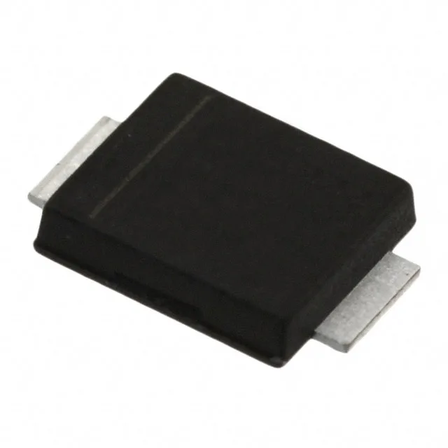
The 75 ns trr keeps switching losses manageable in continuous-conduction-mode PFC stages running above 50 kHz. The SMBflat package (DO-221AA) is a low-profile surface-mount variant — it shares the same 5.4 mm by 3.6 mm footprint as a standard SMB but uses flat leads instead of gull-wing, which reduces standoff height to about 1.0 mm. That matters when the board goes into a sealed enclosure with tight z-axis clearance.
75 ns trr — sizing the snubber and the switching loss budget
The 75 ns reverse recovery time (trr) is measured at standard test conditions (IF = 0.5 A, IR = 1 A, di/dt = 50 A/µs). In a 1000 V boost PFC running at 65 kHz, that recovery charge is low enough that a simple RC snubber across the diode (e.g., 10 Ω + 470 pF) usually cleans up the ringing without adding noticeable loss. If the design runs higher frequency (100 kHz or more), the 75 ns trr still leaves margin, but the forward voltage drop of 1.7 V at 1 A (Vf) contributes more to the thermal budget than the recovery losses — size the heatsinking for the conduction loss first, then add 10–15% for switching.
AEC-Q101 and 175°C junction — where this diode lives
That extra thermal headroom is what lets you run 1 A continuous in a 125°C ambient without derating below 80% of the rated current. For a 48 V to 12 V DC-DC in an EV auxiliary module, that margin can save adding a second parallel diode.
SMBflat footprint — layout gotcha
The SMBflat (DO-221AA) is footprint-compatible with a standard SMB land pattern, but the flat leads have a different solder-paste volume requirement. The lead thickness is about 0.2 mm versus 0.15 mm for a gull-wing SMB, so the stencil aperture should be opened by roughly 10% to ensure a full fillet. Also, the flat leads sit flush against the pad — there is no lead bend to absorb thermal stress, so the board's solder mask defined pad geometry matters more. If the board already uses SMB diodes, the STTH110UFY drops in without a copper change, but the reflow profile may need a 5°C higher peak to wet the thicker lead.