35 ns recovery and 175 °C junction — the switching-loss story
The STTH1002CSFY pairs a 35 ns reverse recovery time with a 1.05 V forward drop at 5 A — the recovery speed keeps the switching loss low in a 100 kHz boost stage, while the Vf sets the conduction loss floor. At 5 A average per diode, the forward dissipation is roughly 5.25 W per die; the TO-277A exposed-pad package pulls that heat into the board copper. Junction temperature is rated to 175 °C, which is the under-hood automotive band — the diode survives the engine-bay thermal cycle without derating the current. Reverse leakage is 4 µA at the 200 V rated voltage — low enough that in a parallel-string rectifier bank the leakage mismatch does not drive thermal runaway. The 200 V Vr rating covers 48 V and 72 V automotive bus transients with margin for the load-dump clamp.
Common-cathode pair for center-tapped and boost topologies
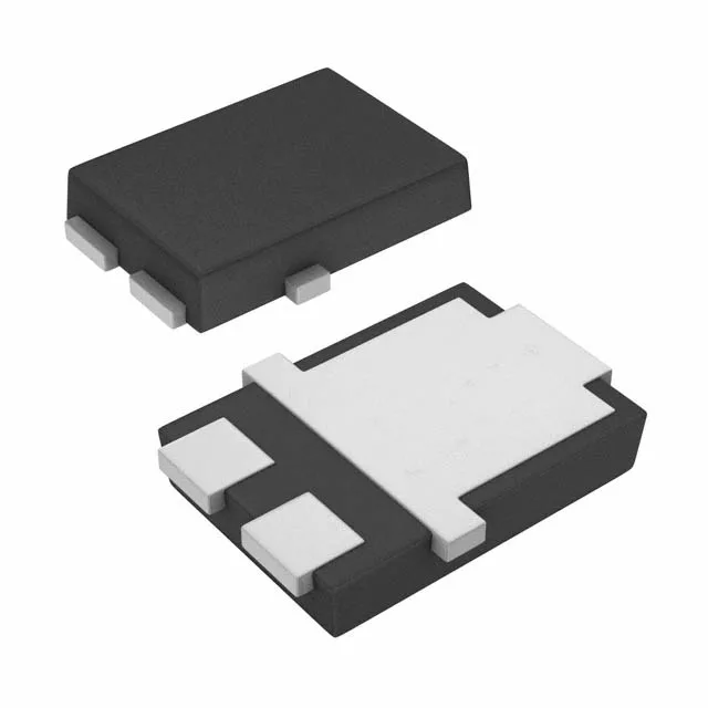
The 1 Pair Common Cathode configuration means the two anodes are separate and the cathodes share a common node — this is the natural fit for a center-tapped full-wave rectifier or a two-phase interleaved boost converter where the cathodes tie to the output rail. Each diode handles 5 A average, so the total package delivers 10 A in a center-tapped secondary with one diode conducting per half-cycle. The TO-277A (SMPC) footprint is a 3-lead PowerDFN with an exposed die-attach pad on the bottom. The pad is the cathode common node — the PCB copper pour under the pad carries both the heat and the output current. The 0.50 mm pitch leads fan out to standard 1.27 mm pad geometry on a two-layer board.