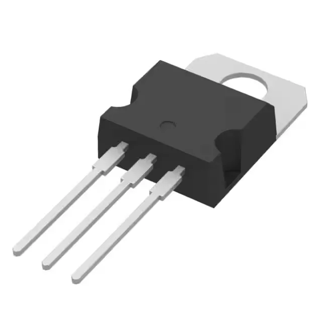
Gate charge and drive — what 13 nC means for your gate-drive circuit
The STP16NF06 specifies a maximum gate charge of 13 nC at 10 V gate voltage. At higher frequencies the 13 nC figure still keeps gate-drive losses modest — a 100 kHz switching rate draws roughly 1.3 mA average from the gate supply, which a standard PWM output from a microcontroller or a simple totem-pole buffer can handle. The input capacitance is 315 pF at 25 V drain-source, consistent with a device designed for moderate-speed switching rather than megahertz-class converters.
On-resistance and thermal design — sizing the heatsink
With a maximum power dissipation of 45 W at case temperature, the device can handle that loss comfortably with a modest heatsink — a TO-220 bolted to a 2–3 °C/W heatsink keeps the junction well below 175°C in still air. If the gate drive voltage drops below 10 V, the on-resistance roughly doubles at 4.5 V, so the design should budget for higher conduction loss when driving from a 5 V logic rail without a gate-drive boost circuit.
For dual-sourcing or supply-chain resilience, the STP16NF06 sits in a well-populated 60 V N-channel TO-220 family; a cross-reference search against the base product number STP16 will surface pin-compatible siblings with similar or higher current ratings.