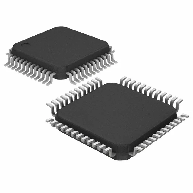
24 MHz 8-bit MCU with 128 KB Flash for industrial control
The 48-pin LQFP package gives you 38 I/O lines, a 10-channel 10-bit ADC, and wired interfaces including I²C, SPI, UART/USART, LIN, and IrDA.
Industrial temperature range and active lifecycle
The operating temperature range is the full industrial span, so it can handle the thermal cycling of a motor drive enclosure or a rooftop sensor node. For a spare-parts storeroom or a production line that needs a stable 8-bit MCU for the next several years, this is a safe pick — no imminent obsolescence to plan around.
What the 24 MHz core and 128 KB Flash mean for your firmware
At 24 MHz, the STM8 core executes most instructions in one or two clock cycles, so you get roughly 12 to 24 MIPS of throughput. That is enough for a PID loop running at 10 kHz, a Modbus RTU slave polling every millisecond, or a simple user interface with a character LCD and a few buttons. The 128 KB Flash is split into 128-byte pages for erase — fine-grained enough for an OTA staging area if you plan field updates, but budget the 2 KB EEPROM separately for calibration constants and fault logs so you do not wear out the Flash sectors. The 6 KB SRAM is modest — a full TCP/IP stack will not fit, but a lightweight protocol like LIN or a custom UART-based command set runs comfortably. If your application needs a large frame buffer or a deep FIFO, you will want to move up to the STM8S with more RAM or step to a 32-bit part.
48-LQFP footprint and layout notes
The 48-LQFP has a 0.5 mm pitch and a 7 mm x 7 mm body — a standard footprint that is easy to route on a two-layer board. Place a 100 nF ceramic cap close to each VDD/VSS pair, and a 4.7 µF bulk cap near the supply entry. The part does not have an exposed thermal pad, so all heat dissipates through the leads; at 24 MHz and 5V operation, the junction temperature stays well below 85°C in still air, but check the thermal impedance if you run the I/O pins at high current.