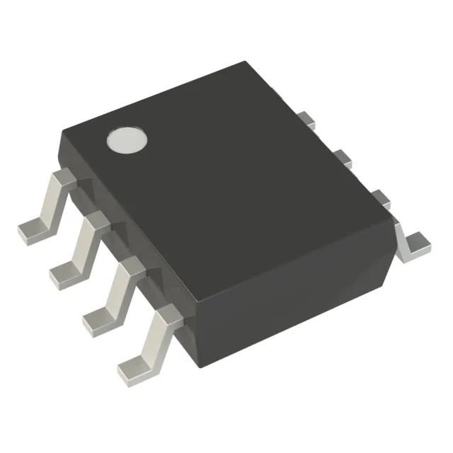
The STM8S001J3M3TR is an 8-bit microcontroller from STMicroelectronics' STM8 family, built around the STM8 core running at 16 MHz.
Memory budget — what 8 KB Flash and 1 KB RAM mean for firmware
With 8 KB of program Flash, 1 KB of SRAM, and 128 bytes of EEPROM, the memory resources on the STM8S001J3M3TR are tight. This is a part for a single, well-defined control loop — a brushless-DC motor commutation sequence, a temperature sensor readout with a PID output, a LIN-bus node in an automotive seat module — not a feature-rich application with a GUI or over-the-air update staging. Firmware must be written to fit within the Flash page boundary, and the 1 KB RAM budget forces careful allocation of stack, global variables, and buffers.
5 I/O pins — routing the peripherals
The 5 I/O pins are the binding constraint on this MCU. These pins must serve double or triple duty: a single pin might be configured as a UART TX, a PWM output, and a GPIO with an external interrupt — but only one function at a time. The I²C, SPI, and UART interfaces share the same physical pins through the alternate-function remap feature, so the designer must decide which serial bus the application needs and configure the pin mux accordingly. For a LIN-bus slave node, the UART plus one GPIO for the LIN transceiver's enable pin consumes two of the five I/O pins, leaving three for sensor inputs or indicator LEDs.
Temperature range and supply — industrial and automotive fit
The wide supply range of 2.95 V to 5.5 V means the same BOM can run from a 3.3 V regulated rail or a 5 V automotive battery line without a level shifter on the MCU power input — though the I/O logic levels follow VDD, so external level translation may still be needed for 5 V peripherals when running at 3.3 V.
For a BOM line, this means no near-term last-time-buy risk and no compliance-driven redesign needed for the foreseeable future.