120 MHz Cortex-M4 with 2 MB Flash — the memory headroom this part brings
The STM32L4S9ZIY6TR: It carries 2 MB of Flash and 640 KB of SRAM, which means you can hold a full application image plus an OTA staging buffer without external memory — a real BOM simplification for connected industrial or IoT edge nodes. The 112 I/O lines, combined with connectivity including CANbus, USB OTG, and multiple SPI/I²C/SAI interfaces, make it a fit for sensor fusion hubs, motor-control gateways, and human-machine interfaces where peripheral count matters.
Package reality: 144-WLCSP
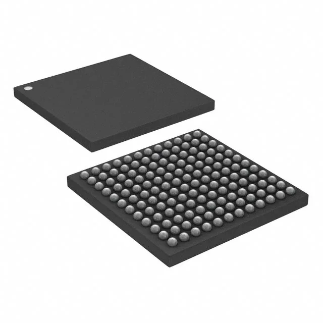
The STM32L4S9ZIY6TR comes in a 144-WLCSP measuring 5.24x5.24 mm — a wafer-level chip-scale package with no leads, just solder balls on the underside. That footprint is about half the area of a comparable LQFP-144, which is the whole point: it fits where board space is tight. The trade-off is that WLCSP requires a controlled SMT process with proper stencil design and X-ray inspection after reflow. Rework is possible but needs a hot-air station with a fine nozzle and a preheat plate; the typical rework lab tech will want to verify the board's solder-mask-defined pad geometry before committing to a repair flow. The package is surface-mount only, and the 5.24 mm body means the mechanical stress from PCB flex is concentrated on the die itself — a stiffener or edge support in the enclosure is worth considering for high-vibration environments.