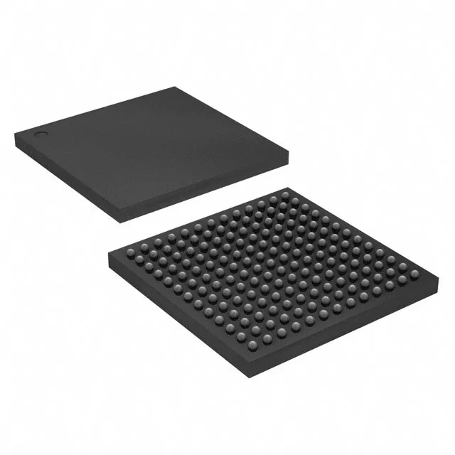
Right-sizing the MCU for a graphics-heavy or sensor-fusion design
The STM32L4R9AGI6: 1 MB Flash and 640 KB SRAM.
The 120 MHz core speed, combined with the FPU and DSP extensions, lets you run FFTs, motor-control loops, or audio processing without a separate DSP. The 640 KB SRAM is split across multiple banks, which helps avoid bus contention when the DMA is hammering the display while the CPU runs the control loop. SWD stays alive even with the watchdog armed. The PLL needs the flash wait state bumped before you raise the core clock, or it hard-faults on the first branch — standard Cortex-M4 bring-up, but worth flagging for anyone new to the STM32L4 series.
169-UFBGA — layout and assembly notes
The 169-UFBGA (7x7 mm) is a fine-pitch BGA. No pinout detail appears in this listing — pull the datasheet for the ball map before starting the layout.