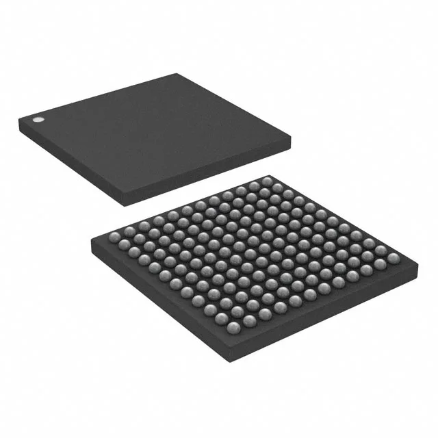
What this STM32L4R5ZGY6TR brings to the board
This is the part you spec when you need a high-density memory footprint and a rich peripheral set — CANbus, USB OTG, multiple I²C and SPI interfaces, plus an EBI/EMI bus for external memory expansion — all on a wafer-level chip-scale footprint that saves board area for compact sensor hubs, wearable gateways, and industrial IoT edge nodes.
120 MHz Cortex-M4 with 1 MB Flash — the compute and memory tier
The 1 MB Flash gives you room for a full RTOS, a graphics stack, or OTA update staging with a fallback image. The 640 KB SRAM is generous for this class — enough to buffer camera frames or hold a large audio pipeline without external RAM. The 115 general-purpose I/O pins, spread across the WLCSP ball grid, let you connect parallel displays, external memory, and multiple sensor buses simultaneously.
144-WLCSP: density trade-off for the PCB layout engineer
STMicroelectronics lists the STM32L4R5ZGY6TR as Active. The base product number is STM32L4R5, so future PCN or die-revision updates will carry that prefix.
Sourcing posture for the shortage-desk buyer
This part is in the active STM32L4R production window, which means franchised distribution carries allocation during tight cycles and independent channels hold excess from over-ordered programmes. The WLCSP package is less commonly overstocked than the LQFP variants — if you see a spot lot, verify date code and bake requirements before committing. For volume production, we quote against an RFQ with current market pricing and confirmed availability. No LTB risk here, but the 144-ball WLCSP means rework cost is higher than a QFP; budget for X-ray inspection on first articles.