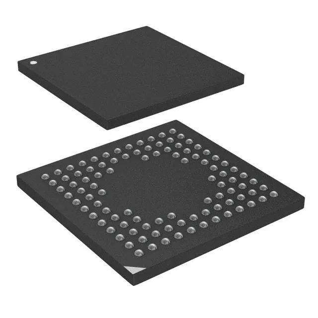
80 MHz Cortex-M4 in a 7x7 BGA — the low-power workhorse
It is built for applications where active compute throughput and standby current both matter — think sensor fusion nodes, portable medical instruments, and battery-operated industrial loggers. The 100-UFBGA (7x7 mm) package packs 83 I/Os into a 0.5 mm pitch ball grid array. That footprint buys you connectivity options — CANbus, I²C, SPI, UART/USART, QSPI, SAI, and MMC/SD — in a board area that would normally hold a smaller-pin-count LQFP. The trade-off is a multi-layer PCB for fanout and a controlled reflow profile; this is not a two-layer-board part.
256 KB Flash, 160 KB SRAM — sizing the firmware budget
256 KB of Flash gives room for a real-time OS, a TCP/IP stack, and application logic without squeezing into the 128 KB tier. The 160K x 8 SRAM (160 KB) is generous for an MCU in this class — enough to hold two full 800x600 frame buffers or a large protocol buffer without external memory. If your application streams audio or runs a GUI with a framebuffer, this part keeps the BOM single-chip.
For a production BOM, this means you are not forced into a bridge-buy or a redesign cycle.
Supply range and temperature — where it runs
The 1.71 V minimum supply is the key detail for battery-powered designs: the MCU stays operational through the full discharge curve of a Li-ion cell down to 3.0 V nominal, with headroom to 3.6 V for USB-powered or regulated rails.