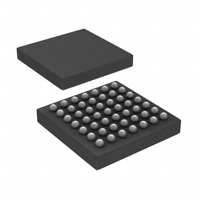
Active production, 80 MHz Cortex-M4 in a 3.14×3.13 mm WLCSP
The 49-WLCSP package (3.14 x 3.13 mm) is the tightest footprint in the STM32L433 line, designed for space-constrained PCBs in wearables, portable medical devices, and IoT edge nodes.
The flash wait state needs bumping to 1 before raising the core clock above 48 MHz, or the first branch hard-faults — a standard clock-tree step during bring-up. The 64K x 8 SRAM gives enough headroom for a FreeRTOS heap, two UART buffers, and a modest audio or graphics frame buffer.
Supply range and brownout margin
The 1.71 V minimum supply is below the 1.8 V typical for many MCUs, which matters when running from a nearly depleted Li-ion cell (cutoff ~2.7 V) or a single alkaline (1.5 V nominal, 0.9 V dead). The brown-out detect/reset peripheral (listed in the peripherals set) can be configured to hold the core in reset until the rail is stable, avoiding corruption on power-up or sag. At 3.6 V max, the part tolerates a 5 V-tolerant USB VBUS only through a regulator — direct connection exceeds the absolute maximum.
The STM32L433CCY6TR includes CANbus, I²C, IrDA, LINbus, MMC/SD, QSPI, SAI, SPI, SWPMI, UART/USART, and USB — enough to interface with most industrial sensors, displays, wireless modules, and memory cards without external bridges. The 39 I/O in the WLCSP package are multiplexed; careful pin assignment in the layout stage avoids conflicts between, say, the LCD segment driver and a high-speed SPI bus.
49-WLCSP: footprint and handling
It saves board area versus a QFP or BGA but requires a stencil with small apertures and a reflow profile tuned for the 0.4 mm ball pitch.