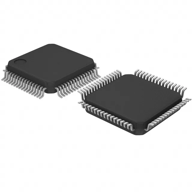
The STM32L052R8T6: The firmware engineer bringing up the clock tree should note that the internal oscillator and Flash access timing are stable across this entire range, but the PLL lock time and brown-out reset threshold (programmable via the BOR peripheral) need to be configured for the minimum operating voltage in the BOM — at 1.65 V the Flash wait state must be set to 1 before enabling the 32 MHz system clock, or the first branch instruction will hard-fault.
Memory map — 64 KB Flash, 8 KB RAM, 2 KB EEPROM
The 2 KB EEPROM is a genuine hardware block with 100k-cycle endurance per byte, which makes it suitable for logging runtime counters or storing device configuration without a separate external EEPROM. The PCB layout engineer should note that the 64-LQFP (10x10 mm) package routes all 51 I/O to the periphery, so decoupling caps can sit close to the Vdd/Vss pairs without crowding the center of the board.
The 16-channel 12-bit ADC and single 12-bit DAC cover basic analog front-end needs — reading a thermistor string or generating an analog setpoint. The USB interface with integrated PHY simplifies adding a USB-to-serial bridge for field firmware updates. The programming interface is SWD (Serial Wire Debug) via the standard 4-pin connector; the SWD pins are not shared with any other function on this package, so the debug port stays alive even if the application firmware locks the GPIOs.
Lifecycle and procurement reality
This part is currently in volume production and is stocked across multiple independent distribution channels. The ROHS3 compliance is current for EU and global markets.