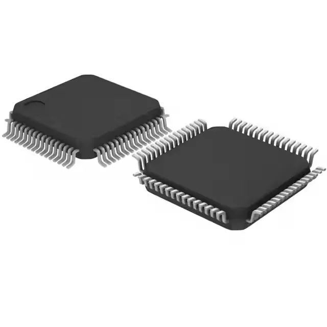
STMicroelectronics STM32H7B3RIT6 — Microcontrollers & Processors (MCU / MPU / DSP)

STM32H7B3RIT6 ARM Cortex-M7 MCU, 280 MHz, 2 MB Flash

MPNSTM32H7B3RIT6
Active

STMicroelectronics STM32H7 Series, ARM Cortex-M7, 32-Bit Single-Core MCU, 280MHz, 2MB (2M x 8) FLASH, 1.4M x 8 RAM, 64-LQFP, -40°C~85°C.

$10.9227Ref. price · indicative, final on quote
StockContact for availability
MOQ1 pcs
  • 100% new & originalTraceable channels only — no refurbs, no pulls, no remarked parts.
  • Date & lot codes on quoteStated per line before you commit; label photos on request.
  • MSL-compliant ESD packingMoisture-sealed bags with indicator cards; reels photo-verified.
  • PayPal buyer protectionPay by T/T, PayPal or Payoneer — card payments covered end to end.

Specifications

STM32H7B3RIT6 Technical Specifications
ParameterValue
SeriesSTM32H7
Mounting typeSurface Mount
Oscillator typeInternal
Program memory typeFLASH
Voltage - supply (Vcc (Vdd))1.62V ~ 3.6V
Operating temperature-40°C~85°C(TA)
Speed280MHz
PackageTray
RAM size1.4M x 8
Core size32-Bit Single-Core
PeripheralsBrown-out Detect/Reset, DMA, I²S, LCD, POR, PWM, WDT
ConnectivityCamera, CANbus, EBI/EMI, HDMI-CEC, I²C, IrDA, LINbus, MDIO, MMC/SD/SDIO, PSSI, SAI, SPDIF, SPI, SWPMI, UART/USART, USB OTG
Number of i (O)49
Core processorARM® Cortex®-M7
Case64-LQFP
Data convertersA/D 16x16b; D/A 3x12b
Program memory size2MB (2M x 8)

Product details

280 MHz Cortex-M7 with 2 MB Flash and 1.4 MB RAM

The STM32H7B3RIT6: ARM Cortex-M7 core at 280 MHz with 2 MB Flash and 1.4 MB RAM in a 64-LQFP package.

What the 280 MHz and memory mean for the BOM

The 280 MHz core clock on the Cortex-M7 with a single-cycle multiply-accumulate and double-precision FPU gives this MCU enough headroom to run a real-time control loop alongside a GUI stack without a separate display controller. The 1.4 MB RAM is unusually large for a 64-pin MCU — enough to hold a full frame buffer for a QVGA LCD or a large audio sample buffer, saving an external SRAM. The 2 MB Flash can store a second-stage bootloader plus application code with room for OTA image staging. For designs that need to log data or run complex state machines, this memory sizing means you can skip external memory entirely in many cases.

Connectivity and peripheral count in a 64-pin package

The trade-off is pin multiplexing — you cannot enable every peripheral simultaneously with 49 I/O. For a motor-drive design that needs CAN, encoder inputs (via timer channels), and a UART debug port, the pinout works. The EBI/EMI interface, if used, consumes a significant number of pins, so plan the pin allocation early in schematic capture.

The supply range from 1.62 V to 3.6 V covers both 1.8 V and 3.3 V logic rails, and the 1.62 V minimum is low enough to run from a single Li-ion cell near end-of-discharge. The internal POR and brown-out reset handle power-up sequencing cleanly, reducing external supervisor IC cost.

Lifecycle and sourcing

This is a mainstream STM32H7 variant, so supply through the independent channel is consistent. There is no LTB risk on this line today.

Frequently asked questions

What is the difference between STM32H7B3RIT6 and STM32H7B3IIT6?

The primary difference is the package: STM32H7B3RIT6 comes in a 64-LQFP, while the STM32H7B3IIT6 is in a 176-LQFP with more I/O and a larger footprint. The core, memory, and speed are the same.

Can STM32H7B3RIT6 be used for real-time control applications?

Yes, the 280 MHz Cortex-M7 with FPU, combined with the rich timer and PWM peripherals, makes it suitable for real-time motor control, power conversion, and servo loops. The 1.4 MB RAM provides ample buffer space for control data.