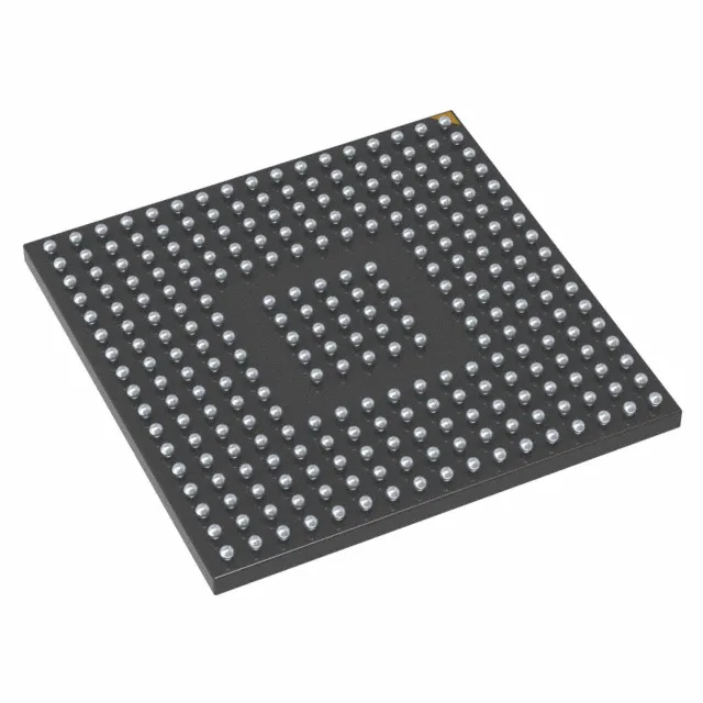
The STM32H745IGK6 pairs a 240 MHz Cortex-M4 with a 480 MHz Cortex-M7 on a single die, giving you a real-time control core and a high-performance application core that can run separate code images. The M7 handles number-crunching or protocol stacks; the M4 takes deterministic I/O and low-latency interrupt service. Both share the 1 MB Flash and 1 M x 8 RAM, so the memory budget needs to cover both firmware partitions.
Flash and RAM — sizing the firmware split
The M7 typically runs the main application and can chew through Flash quickly; the M4 handles housekeeping and real-time loops. The 128 I/O count gives plenty of headroom for parallel buses, display interfaces, and sensor arrays — the 176+25 UFBGA (10x10 mm) packs it all into a compact BGA that needs fine-pitch assembly but saves board area.
Temperature range and supply — industrial fit
The supply range of 1.62 V to 3.6 V lets it run from a single 3.3 V rail or a 1.8 V core supply with separate I/O voltage — flexible for mixed-voltage designs.
Connectivity and peripherals — what is on the bus
The 36-channel 16-bit ADC and dual 12-bit DAC handle analog front-end tasks without an external converter. Internal oscillator means you can boot without a crystal, though an external clock improves accuracy for time-sensitive protocols like Ethernet or USB.
ST lists the STM32H745IGK6 as Active. For new designs this is a green light; for production lines the supply channel is stable through independent distribution.