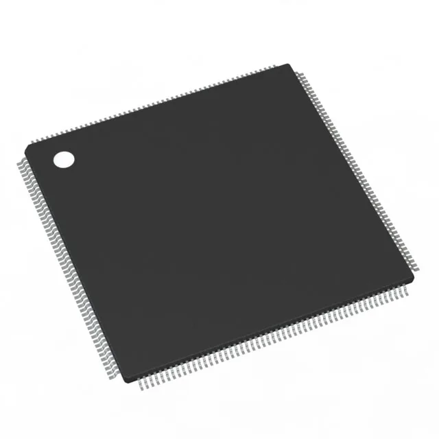
Dual-core architecture — partition the workload early
The STM32H745BGT6 pairs a 240 MHz Cortex-M4 with a 480 MHz Cortex-M7 on a single die. That speed split is the headline feature: the M7 handles number-crunching and communications stacks (Ethernet, USB OTG), while the M4 runs real-time control loops and peripheral housekeeping. Map the memory interfaces first — 1 MB Flash and 1 MB RAM are shared between cores, so firmware partitioning and inter-core communication (via the HSEM hardware semaphore) need to be settled before layout. The 208-LQFP (28x28 mm) package is large enough for manual rework but takes up board real estate; plan for a 4-layer minimum to route the 148 I/O cleanly.
Connectivity — gateway between fieldbus and IP networks
Ethernet MAC plus CANbus and USB OTG make this SoC a natural bridge between legacy fieldbus segments and IP backbones. The EBI/EMI interface can connect an external SRAM or NOR Flash for larger data buffers — useful if the 1 MB internal RAM is tight for dual-core frame stores. QSPI supports memory-mapped external Flash for code execution or data logging. Compared to a single-core STM32H7 variant, the dual-core split lets you run a real-time motor control loop on the M4 while the M7 handles TCP/IP and HMI rendering without scheduler jitter.