170 MHz Cortex-M4F with FPU — the control-loop workhorse
The STM32G474QET3: Program memory is 512 KB of Flash, paired with 128 KB of SRAM. That Flash footprint fits a full motor-control stack (sensorless observer, PI regulators, field-weakening) plus a CANopen or Modbus communication stack, with room left for a bootloader and OTA update staging area. The 128 KB SRAM gives headroom for multiple ADC result buffers, DMA descriptor tables, and real-time data logging without spilling to external memory. The analog front end is unusually dense: 42 channels of 12-bit ADC and 7 channels of 12-bit DAC. In a three-phase motor drive, that means you can sample all three phase currents, the DC-link voltage, and a temperature sensor simultaneously, while the DACs output analog reference signals or current-setpoint voltages for external amplifiers. The ADC can be triggered by the timer PWM outputs, eliminating CPU jitter in the sampling instant.
Temperature range and package — designed for the panel, not the lab bench
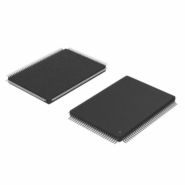
The 128-LQFP package (14x14 mm body) with 107 accessible I/O pins gives enough routing channels for parallel encoder interfaces, multiple SPI Flash chips, and a parallel LCD or external SRAM bus if needed. The LQFP package is a standard JEDEC footprint — no BGA routing complexity, no hidden vias under the package. That keeps the PCB cost down and makes manual inspection and rework straightforward.
Peripheral set — what connects to what
Connectivity includes CANbus (two FD-capable controllers typically), I²C, SPI, UART/USART with IrDA and LIN support, and a Quad-SPI interface for external Flash or PSRAM. The QSPI is useful for storing large lookup tables or bootloader images without consuming main Flash. DMA covers all major peripherals, so the CPU can run control loops while data moves between ADC, SPI Flash, and UART in the background. The PWM timers are the high-resolution type with dead-time insertion, complementary outputs, and brake input — essential for three-phase inverter drives. Brown-out detect and POR are integrated, so an external supervisor is optional unless you need a precise reset threshold or a watchdog with independent clock. The internal oscillator is accurate enough for UART and CAN at room temperature, but for motor control PWM synchronization, an external crystal or oscillator is recommended to avoid frequency drift over temperature.
Lifecycle — active, no end-of-life shadow
The base product number is STM32G474, so any PCN or errata updates are tracked under that family umbrella.
This part is supplied in a Tray package and is a standard catalog item from ST.