64 MHz is the ceiling for this part, and the Cortex-M0+ pipeline delivers roughly 0.95 DMIPS/MHz, so you get about 60 DMIPS of integer throughput. That is enough for real-time control loops (brushless-DC commutation, closed-loop PID at a few kHz), protocol parsing (Modbus RTU, CANopen frames), and sensor fusion running at moderate sample rates. The 8 KB SRAM is tight — budget about 2 KB for the stack and RTOS kernel, leaving 6 KB for application data. If your firmware needs a large lookup table or double-buffered ADC buffer, the 64 KB Flash can hold constants, but the RAM ceiling will force either an external SRAM or a move to a higher-density sibling.
Peripherals and I/O — what hooks onto the bus
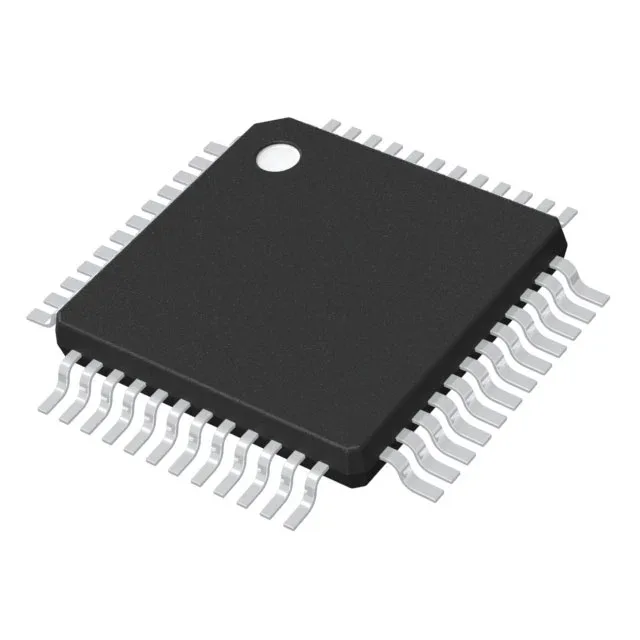
This MCU includes a 12-bit ADC with 19 channels (enough to monitor a three-phase motor current plus a few thermistors), a brown-out detect and power-on-reset block, a DMA controller for moving ADC results without CPU intervention, and an I²S interface for audio or serial-memory streaming. The 44 I/O pins are available in the 48-LQFP package; roughly 32 survive as GPIO after peripheral muxing in a typical design. The internal oscillator eliminates the crystal for many applications, but if you need tighter timing for USB or CAN, an external clock can still be fed in.
The base product number is STM32G041, and the full family includes pin-compatible density variants (e.g., 32 KB Flash) if you later need to cost-reduce or upgrade firmware capacity while keeping the same PCB layout.
Package and footprint — layout notes
The 44 I/O are arranged around the perimeter; no fine-pitch BGA alignment issues here.