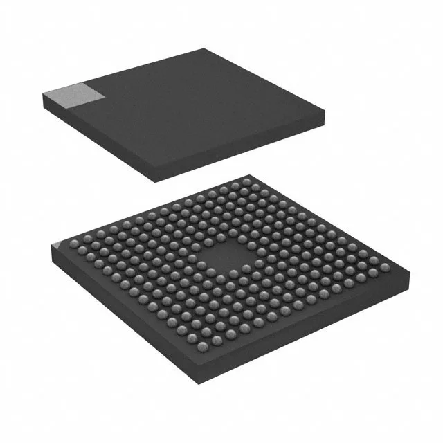
It belongs to the STM32F7 series, a high-performance line aimed at applications that need a balance of processing throughput and peripheral integration — think industrial HMI panels, motor-control gateways, or camera-based vision systems that also carry Ethernet and CANbus traffic.
The 216 MHz core clock is the highest in the STM32F7 value line and gives this part enough headroom to run a real-time OS, process a camera frame buffer, and handle Ethernet TCP/IP stacks without a separate communications processor. At this speed, flash wait states matter — the ART Accelerator in the F7 series reduces that penalty, but the designer should budget for the 1 MB Flash to be split across multiple sectors for OTA update staging.
Peripheral set — Ethernet, CAN, LCD, and more
The 168 I/O pins, spread across the 216-ball TFBGA, give enough GPIO for a parallel RGB display plus external memory or sensor buses.
216-TFBGA package — rework and layout notes
It needs a controlled reflow profile, X-ray inspection after assembly, and a PCB with via-in-pad or microvia capability to route all 168 I/O.
For BOM planning, the base product number STM32F756 covers a family of density and package variants; the NGH6 suffix identifies this specific 216-ball TFBGA version.