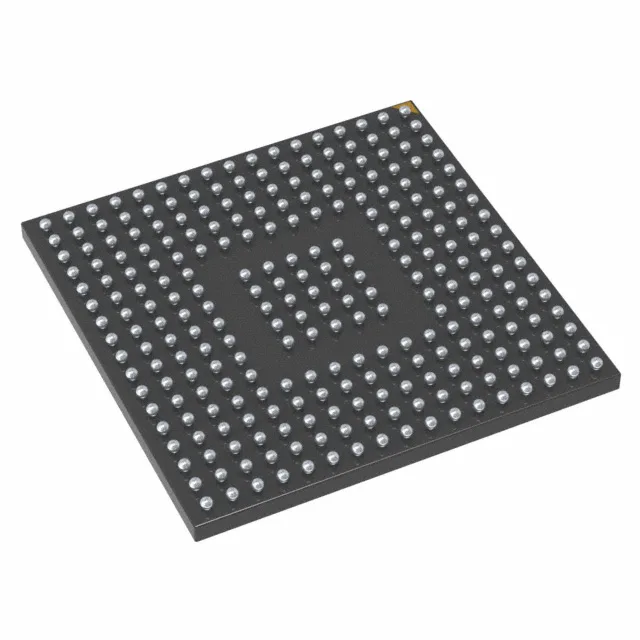
STM32F745IEK7TR — 216MHz ARM Cortex-M7 MCU, 512KB Flash, 140 I/O, UFBGA
STMicroelectronics STM32F7 series ARM Cortex-M7 MCU, order code STM32F745IEK7TR; 216MHz single-core, 512KB Flash, 320KB SRAM, 140 I/O, USB OTG, Ethernet, CAN, 24x12-bit ADC / 2x12-bit DAC; 1.7–3.6V supply, -40°C to 105°C TA; 201-UFBGA surface mount in tape and reel.
- 100% new & originalTraceable channels only — no refurbs, no pulls, no remarked parts.
- Date & lot codes on quoteStated per line before you commit; label photos on request.
- MSL-compliant ESD packingMoisture-sealed bags with indicator cards; reels photo-verified.
- PayPal buyer protectionPay by T/T, PayPal or Payoneer — card payments covered end to end.
Specifications
| Parameter | Value |
|---|---|
| Series | STM32F7 |
| Mounting type | Surface Mount |
| Oscillator type | Internal |
| Program memory type | FLASH |
| Voltage - supply (Vcc (Vdd)) | 1.7V ~ 3.6V |
| Operating temperature | -40°C ~ 105°C (TA) |
| Speed | 216MHz |
| Package | Tape & Reel (TR) |
| RAM size | 320K x 8 |
| Core size | 32-Bit Single-Core |
| Peripherals | Brown-out Detect/Reset, DMA, I²S, POR, PWM, WDT |
| Connectivity | CANbus, EBI/EMI, Ethernet, I²C, IrDA, LINbus, SAI, SD, SPDIF-Rx, SPI, UART/USART, USB OTG |
| Number of i (O) | 140 |
| Core processor | ARM® Cortex®-M7 |
| Case | 201-UFBGA |
| Data converters | A/D 24x12b; D/A 2x12b |
| Program memory size | 512KB (512K x 8) |
Frequently asked questions
What thermal derating applies at 216MHz in a sealed panel at 85°C ambient?
The STM32F745IEK7TR is rated at -40°C to 105°C TA with 216MHz maximum clock. The 201-UFBGA package's thermal resistance depends on your pad stack and board design; the STM32F7 reference manual provides theta-JA data for thermal modelling. Sustained full-speed operation at 85°C ambient in a sealed IP54 enclosure leaves limited junction headroom — the internal voltage regulator throttles before hard shutdown, but firmware must handle the fault response deterministically.
Can Ethernet and USB OTG run simultaneously without losing a DAC output?
The 2×12-bit DAC outputs and the USB PHY pins are on separate signal paths. Simultaneous operation is architecturally possible, but the GPIO pin budget is finite with 140 I/O and alternate function assignments are pin-specific — confirm your board netlist against the STM32F7 pin assignment tables to verify the DAC pins are not consumed by the Ethernet PHY interface you have selected.
What is the maximum contiguous DMA buffer size with Ethernet, CAN, and SDIO all active?
320KB of SRAM is split across SRAM1, SRAM2, and AHB SRAM on this die. The maximum contiguous DMA buffer depends on how the memory map is partitioned and whether the Ethernet, CAN, and SDIO instances are assigned to SRAM1, SRAM2, or AHB SRAM — each peripheral has a preferred DMA target. The STM32F7 reference manual documents the memory map and DMA controller assignments; the specific contiguous block size for your configuration is determined by the firmware's memory layout, not a fixed datasheet figure.