256 KB RAM and 2 MB Flash — sizing the firmware and data buffers
The 2 MB Flash is organised as 2M x 8 bits, large enough to hold a full-featured RTOS, TCP/IP stack, graphics library, and application code with room left for OTA update staging. The 256 KB RAM supports multiple frame buffers for a QVGA display or a moderate-size data acquisition ring buffer. If your design uses the Ethernet controller or the USB OTG, budget some RAM for the descriptor rings and FIFOs — the 256 KB still leaves headroom for the application heap.
Connectivity and peripherals — what is on the chip
The peripheral set includes a 12-bit ADC with 24 channels and a 12-bit DAC with 2 channels, internal oscillator, brown-out detect, POR, PWM timers, and a watchdog.
There is no last-time-buy window on the horizon, and the base product number STM32F427 remains a mainstream STM32F4 offering. ROHS3 compliant, which covers the EU RoHS directive without exemptions. No separate PCN or EOL notice has been issued for this specific order code.
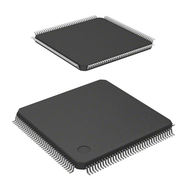
Package and mounting — 144-LQFP with 20x20 mm body
The supplier device package code is 144-LQFP (20x20). Standard reflow profiles for LQFP apply;
For volume production commitments, the active lifecycle means no allocation concerns from end-of-life — but lead times can vary by market conditions; a firm RFQ locks the delivery window.