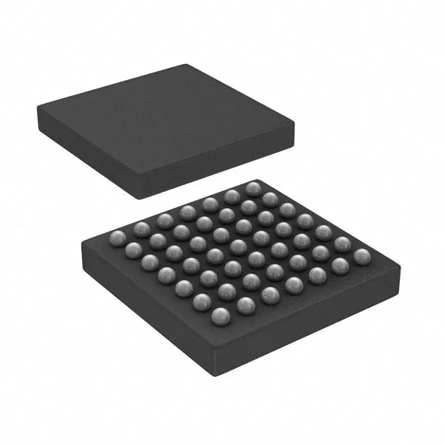
It packs 512 KB of Flash and 128 KB of SRAM — enough for a moderate application stack with OTA staging or data logging buffers. The 49-WLCSP (3x3.19 mm) package is the smallest footprint in the STM32F411 line, suited for wearable, sensor-node, or portable designs where board area is tight.
The 100 MHz core with FPU and DSP instructions handles FFTs, motor-control PID loops, or audio processing without the cycle-count anxiety of a Cortex-M3 at similar clock rates.
49-WLCSP — design-in checklist
The 49-WLCSP (3x3.19 mm) is a fine-pitch, lead-free package with 0.4 mm ball pitch. The 36 I/Os include I2C, SPI, UART/USART, USB OTG, and SDIO interfaces, covering most sensor and display connectivity needs.
It is ROHS3 compliant. For production planning, this means no forced redesign cycle from obsolescence in the near term. The base product number STM32F411 covers multiple density and package variants, so a pin-compatible migration to a larger Flash or different package is possible within the family if requirements change.