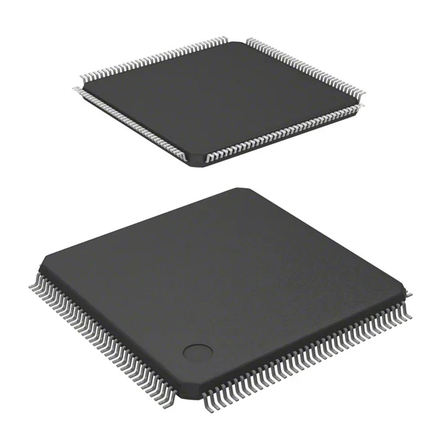
The 144-LQFP package gives access to 115 I/O lines, enough for multiple encoder interfaces, parallel display buses, or a bank of PWM outputs.
The Cortex-M4 core with single-precision FPU is the key differentiator versus the Cortex-M3 used in the STM32L1 series. At 72 MHz, a 32-bit floating-point multiply-accumulate completes in one cycle, not a software-emulated sequence. For a field-oriented motor control loop running at 16 kHz, that saves several microseconds per iteration — headroom you can spend on higher PWM resolution or additional sensor filtering. The 512 KB Flash is organised as 512 K x 8, with the usual STM32F3 sector layout for wear-leveled firmware updates. The 80K x 8 SRAM (80 KB) supports moderate-sized data buffers, TCP/IP stacks, or double-buffered ADC results without external memory.
The base product number is STM32F303, so pin-compatible density variants (e.g., 256 KB Flash, 48 KB SRAM) share the same 144-LQFP footprint if a cost-reduced or higher-memory spin is needed later.
Package and supply rails for the board layout
The 144-LQFP package (20 x 20 mm body, 0.5 mm pitch) is a common footprint for mid-density MCUs.