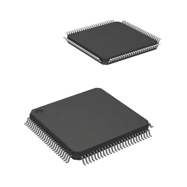
STMicroelectronics STM32F105VCT6 — Microcontrollers & Processors (MCU / MPU / DSP)

STMicroelectronics STM32F105VCT6 ARM Cortex-M3 MCU, 72 MHz

MPNSTM32F105VCT6
Active

STMicroelectronics STM32F105VCT6, STM32F1 Connectivity line, 32-bit ARM Cortex-M3 MCU, 72 MHz, 256 KB Flash, 64 KB SRAM, USB OTG, dual CAN, 80 I/O, 100-LQFP, -40 to 85°C.

$9.7500Ref. price · indicative, final on quote
Packaging100-LQFP
RoHSROHS3 Compliant
SeriesSTM32F1
Independent supplier — new & surplus stockAuthenticity-screened · ESD-safe packingListing updated Aug 2026

Specifications

STM32F105VCT6 specifications
ParameterValue
SeriesSTM32F1
MountingSurface Mount
Oscillator typeInternal
Program memory typeFLASH
Voltage - supply (Vcc (Vdd))2V ~ 3.6V
Operating temperature-40°C ~ 85°C (TA)
Speed72MHz
PackageTray
RAM size64K x 8
Core size32-Bit Single-Core
PeripheralsDMA, POR, PWM, Voltage Detect, WDT
ConnectivityCANbus, I²C, IrDA, LINbus, SPI, UART/USART, USB OTG
Number of i (O)80
Core processorARM® Cortex®-M3
Case100-LQFP
Data convertersA/D 16x12b; D/A 2x12b
Program memory size256KB (256K x 8)

Product details

72 MHz Cortex-M3 with USB OTG and dual CAN — the Connectivity line MCU

The distinguishing feature versus the value-line STM32F103 is the USB OTG peripheral with an on-chip PHY and dual CAN 2.0B interfaces, which saves an external USB controller and a CAN transceiver on the BOM. With 80 I/O lines in a 100-LQFP package, it is sized for industrial gateways, motor drives with fieldbus, and building automation controllers that need to bridge a CAN network to a USB host.

The 256 KB program Flash and 64 KB SRAM define the firmware boundary. A typical application running FreeRTOS, a CANopen stack, and a USB CDC class driver leaves about 80 KB of Flash and 20 KB of RAM free for application code and buffers. The Flash is organized as 256 K x 8 bits with 2 KB and 64 KB erase sectors, which matters when sizing the OTA update staging area.

USB OTG and dual CAN — what the connectivity means on the bus

The STM32F105VCT6 carries a USB OTG full-speed (12 Mbps) peripheral with an integrated PHY — no external USB transceiver needed. The dual CAN 2.0B controllers share a single 512-byte mailbox RAM. In a typical gateway design, one CAN port handles the fieldbus (e.g., CANopen at 250 kbps) while the second CAN port bridges to a secondary bus or a diagnostic tool. The USB OTG can act as a device (virtual COM port) or as a host (flash drive for data logging). Both CAN and USB can run concurrently without stalling the core, provided the DMA controller is configured for the peripheral FIFOs.

Industrial temperature range and 100-LQFP package

The 100-pin LQFP (14 x 14 mm, 0.5 mm pitch) is inspectable and reworkable with standard hot-air tools. No exposed pad — all thermal dissipation goes through the leads.

Frequently asked questions

Is STM32F105VCT6 obsolete or end-of-life?

No. It is still in the current STM32F1 portfolio and available through standard distribution.

How does STM32F105VCT6 compare to STM32F107VCT6?

The STM32F107VCT6 is the same die in the same 100-LQFP package but adds a 10/100 Ethernet MAC with dedicated DMA. Both share 72 MHz Cortex-M3, 256 KB Flash, 64 KB SRAM, USB OTG, and dual CAN. If the design needs an Ethernet port, the STM32F107VCT6 saves an external MAC/PHY chip. If no Ethernet is required, the STM32F105VCT6 is the cost-optimized choice.

Can I use STM32F103VCT6 as a replacement for STM32F105VCT6?

However, it lacks the USB OTG peripheral and has only one CAN controller instead of two. If the design uses neither USB OTG nor dual CAN, the STM32F103VCT6 is a drop-in replacement. If the design relies on USB OTG or the second CAN port, the STM32F103VCT6 will not work.

What programming tools and debuggers support STM32F105VCT6?

The STM32F105VCT6 uses the standard ARM Serial Wire Debug (SWD) interface. Any debugger that supports Cortex-M3 SWD — such as ST-Link/V2, J-Link, or CMSIS-DAP — can program and debug this MCU. STMicroelectronics provides the STM32CubeIDE and STM32CubeProgrammer toolchain free of charge.