Cortex-M0 MCU for cost-sensitive control applications
Connectivity covers I2C, SPI, UART/USART, LINbus, IrDA, and HDMI-CEC, making it a fit for appliance control panels, lighting ballasts, and compact motor drives.
At 48 MHz the Cortex-M0 executes a single-cycle multiply and delivers 0.9 DMIPS/MHz, so a tight 10 kHz current-loop PID runs with margin for communications overhead. The 64 KB Flash is organized as 64K x 8 with 8 KB of SRAM. That RAM budget constrains buffering for SPI or UART data streams — a 1 KB ring buffer for each of three serial ports leaves 5 KB for stack and variables, which is workable for a single-control-loop design but tight for a TCP/IP stack.
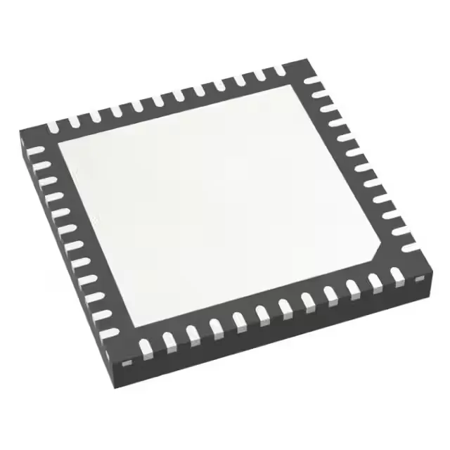
48-UFQFN with exposed pad — layout and rework notes
The pad also serves as the primary electrical ground return — skipping the via stitch will cause the junction to climb above 85°C at sustained 50 mA I/O drive. Reworking this package under hot air is manageable: preheat the board to 120°C, apply flux, and lift at 320°C with a nozzle matching the 7x7 mm outline.
Supply voltage and power rail design
At 2.0 V the 48 MHz PLL still locks, but Flash access requires one wait state below 2.4 V — the core clock must be reduced or the supply held above that threshold for full-speed operation.
Active lifecycle — no EOL concern for new designs
This makes it safe to qualify for a new BOM without planning a last-time buy or a pin-compatible migration. ROHS3 compliance is confirmed, so it passes EU and global material-restriction requirements without a waiver. The base product number STM32F051 covers a density family, so firmware and PCB layout can scale across Flash and RAM variants within the same 48-UFQFN footprint.