The 48 MHz core speed is the ceiling for this part; the Cortex-M0 pipeline executes most instructions in a single cycle, so a tight control loop reading a 12-bit ADC sample and updating a PWM duty cycle finishes in under a microsecond.
Memory map and firmware footprint
32 KB of Flash (32K x 8) and 4 KB of SRAM (4K x 8) define the firmware and data budget. That Flash holds a modest bootloader plus application code for a single-purpose controller — a BLDC commutation routine, a LIN slave stack, or a simple sensor fusion filter. The 4 KB SRAM leaves room for a few hundred bytes of stack and a double-buffered ADC result array; anything needing larger frame buffers or a TCP/IP stack moves up to the STM32F1 or STM32L4 family.
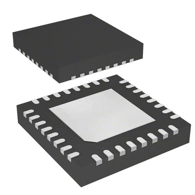
The exposed pad is the only thermal path; the small QFN leads carry negligible heat.
ROHS3 compliant.