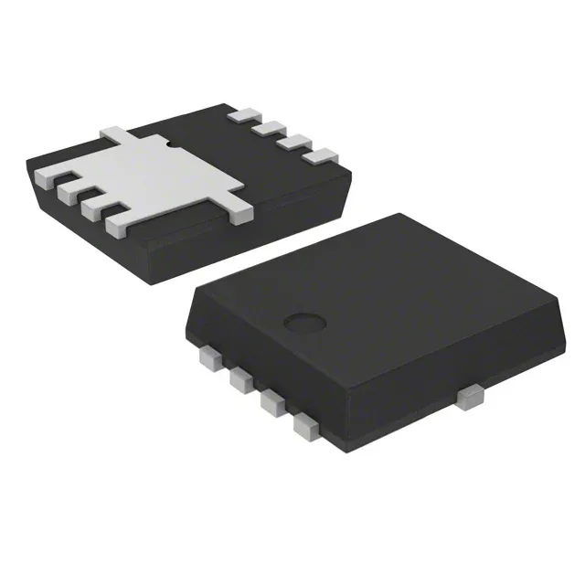
P-channel 40 V switch in a 3.3x3.3 PowerFlat package
It comes in a PowerFlat 3.3x3.3 surface-mount package, which keeps the footprint small while the exposed pad handles thermal dissipation.
20.5 mOhm on-resistance — the number that decides the load budget
That figure sets the conduction loss floor for a load switch or battery isolation circuit — at 4 A the I²R loss is about 0.33 W, well within the 2.9 W power dissipation limit at ambient. The gate threshold is 2.5 V maximum at 250 µA, so logic-level drive at 4.5 V turns it on fully, though the lowest Rds(on) is achieved at 10 V.
Total gate charge is 22 nC at 4.5 V. A small gate-driver IC or a GPIO with a series resistor can switch this FET at tens of kHz without excessive drive current. The input capacitance is 2850 pF at 25 V drain-source, which sets the switching energy per cycle — a consideration if the design runs above 100 kHz.
It is ROHS3 compliant.