Total gate charge is 13 nC at 4.5 V, which means a standard 1 A gate driver can switch this FET in about 13 ns. Low Qg also reduces cross-conduction losses in half-bridge topologies where dead time is tight.
Package and mounting — PowerFlat with wettable flanks
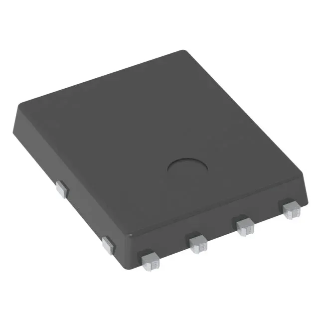
The 8-lead PowerFlat (5x6 mm) package uses wettable flanks, which means the side pads are solderable — this allows automated optical inspection (AOI) of the solder joints after reflow, a requirement for automotive-grade assembly.
Active production and compliance status
It is ROHS3 compliant and qualified to AEC-Q101, so it meets the automotive stress-test requirements for temperature cycling, high-temperature reverse bias, and humidity.