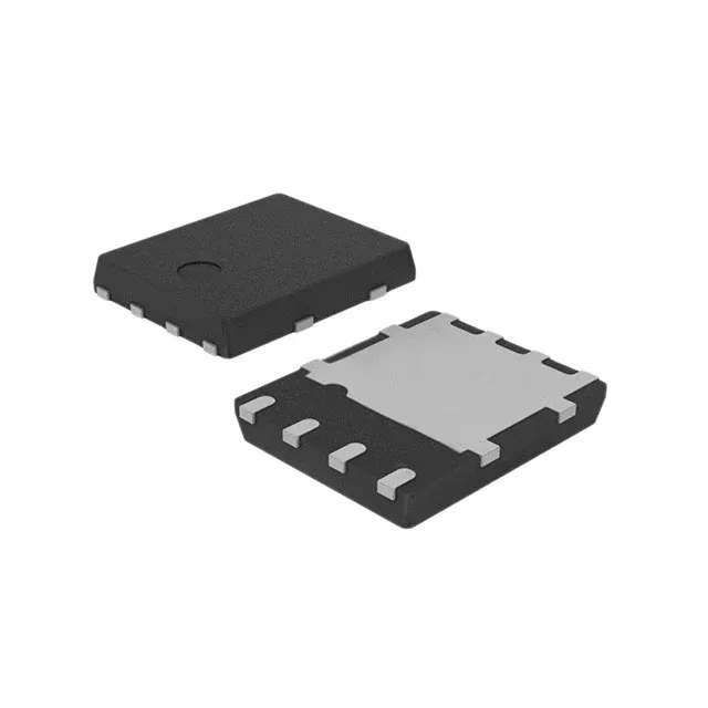
600 V N-channel in a 3.3 mm square footprint
The PowerFlat™ 3.3x3.3 mm package (8-PowerVDFN) is a compact surface-mount body with an exposed drain pad — the thermal path runs through the PCB copper, so the layout's drain-tab copper area and via count directly set the junction-to-ambient thermal resistance.
The 1.8 Ohm Rds(on) at 10 V gate drive is high enough that continuous conduction at 650 mA dissipates about 0.76 W — within the 2 W (Ta) power dissipation limit, but leaving little headroom for ambient above 70 °C. The total gate charge of 9.5 nC at 10 V means a standard 1 A gate driver can switch this FET in under 100 ns without excessive drive loss. Input capacitance is 188 pF at 50 V drain bias — a low value that keeps the Miller plateau short and reduces switching losses in a hard-switched topology like an offline flyback clamp or an active snubber.
No official successor or second-source cross-reference is published by ST.