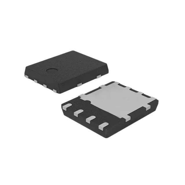
800 V N-channel in a 5x6 PowerFlat — auxiliary supply switch
It is housed in an 8-PowerVDFN package — the PowerFlat 5x6 mm footprint with an exposed pad that sinks heat to the PCB copper plane. This part is designed for high-voltage DC-DC converters, flyback auxiliary supplies, and PFC stages where the primary switch sees 800 V peak on the drain node.
4.9 Ohm Rds(on) and 3 nC gate charge — conduction loss and drive budget
On-resistance is specified at 4.9 Ohm maximum with 10 V gate drive at 1 A drain current. At 2 A full load the conduction loss is under 20 W, which the 33 W package dissipation can handle with adequate copper area on the drain pad. Gate charge totals 3 nC at 10 V — low enough that a PWM controller's output pin can drive the gate directly without a separate driver IC, saving a component and board space in compact bias supplies.
The 150°C maximum junction allows headroom for derating in a 105°C ambient environment. Input capacitance is 95 pF at 100 V drain bias, keeping switching losses low at frequencies up to several hundred kilohertz.