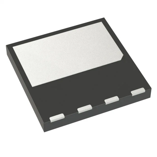
600 V N-channel in a PowerFlat HV package
It comes in an 8-lead PowerFlat™ (8x8) HV surface-mount package — an exposed-paddle VDFN that pulls heat through the PCB copper pour.
At 215 mOhm max at 10 V gate bias, the conduction loss at 7.5 A is about 12 W — well within the 110 W power dissipation rating at case temperature. The 24 nC gate charge keeps the gate-drive energy per cycle low, which matters when the switching frequency pushes past 100 kHz in a LLC or phase-shifted full bridge. The 4.75 V maximum gate threshold at 250 µA means a 10 V gate drive is needed to achieve the rated Rds(on); a 5 V logic-level drive will not fully enhance the channel.
Package and rework — PowerFlat HV realities
The PowerFlat™ (8x8) HV is a large-paddle VDFN with an exposed copper slug on the bottom. During rework, preheat the board to 125°C before hitting the package with hot air; the large paddle soaks heat fast and can delaminate the die attach if the profile is too aggressive. The package is surface-mount only. The 8x8 mm footprint is standard for this PowerFlat family, so the stencil aperture for the paddle should be a grid of smaller openings to avoid solder voids.
It is ROHS3 compliant.