Gate charge and switching loss — 29 nC at 10 V
Total gate charge is 29 nC at 10 V, which keeps the gate-drive energy per cycle low enough that a standard 1 A driver can switch the FET at 100 kHz without excessive dissipation in the driver IC. The input capacitance is 1060 pF at 100 V drain-source, a figure that directly sets the turn-on delay and the driver's peak current requirement.
PowerFlat (8x8) HV — thermal and footprint considerations
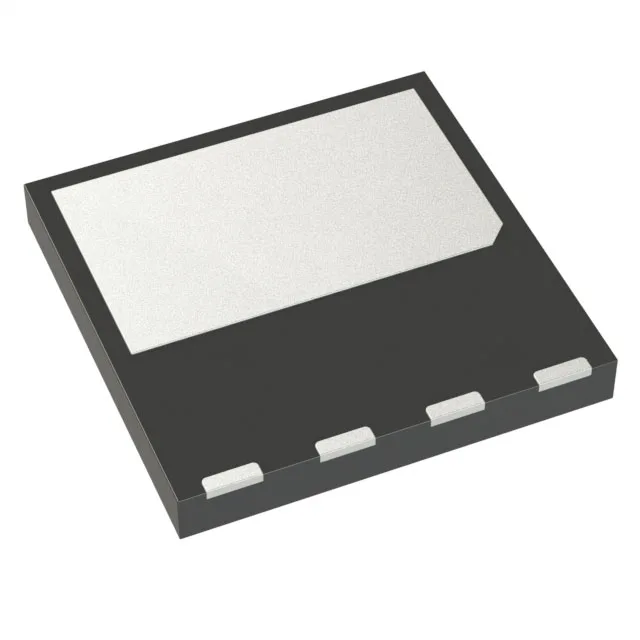
The 8-PowerVDFN package, branded PowerFlat (8x8) HV, exposes a large bottom-side pad for heat sinking. With a maximum power dissipation of 125 W at case temperature, the PCB copper area under the pad and the via array to the inner-layer planes determine the junction-to-ambient thermal resistance.
