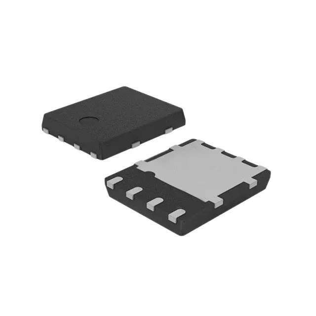
STMicroelectronics STL10N3LLH5

STL10N3LLH5 MOSFET N-Ch 30V 9A PowerFlat, 19mOhm Rds(on)

MPNSTL10N3LLH5
End of Life

STMicroelectronics STripFET™ V N-Channel MOSFET, STL10N3LLH5, 30V Vdss, 9A Id, 19mOhm Rds(on) max at 4.5A/10V, 6nC Qg, 8-PowerVDFN PowerFlat 3.3x3.3mm, -55°C to 150°C.

$1.1Ref. price · indicative, final on quote
Packaging8-PowerVDFN
StockContact for availability
MOQ1 pcs
  • 100% new & originalTraceable channels only — no refurbs, no pulls, no remarked parts.
  • Date & lot codes on quoteStated per line before you commit; label photos on request.
  • MSL-compliant ESD packingMoisture-sealed bags with indicator cards; reels photo-verified.
  • PayPal buyer protectionPay by T/T, PayPal or Payoneer — card payments covered end to end.

Specifications

STL10N3LLH5 Technical Specifications
ParameterValue
SeriesSTripFET™ V
FET typeN-Channel
Mounting typeSurface Mount
Drain to source voltage30 V
Drive voltage (Max rds on, min rds on)4.5V, 10V
Current - continuous drain (Id) @ 25°C9A (Tc)
Power dissipation2W (Ta), 50W (Tc)
Operating temperature-55°C ~ 150°C (TJ)
PackageTape & Reel (TR); Cut Tape (CT)
Vgs±22V
TechnologyMOSFET (Metal Oxide)
Case8-PowerVDFN
Vgs(th) (Max) @ id2.5V @ 250µA
Rds on (Max) @ id, vgs19mOhm @ 4.5A, 10V
Gate charge (Qg) (Max) @ vgs6 nC @ 4.5 V
Input capacitance (Ciss) (Max) @ vds900 pF @ 25 V

Product details

30V N-channel switch for 12V rails

It is built for low-voltage DC-DC conversion, load switching, and battery management in the 5V to 12V range — the 30V Vdss gives headroom on a 12V rail without forcing a larger package.

On-resistance and gate charge — switching loss budget

Maximum Rds(on) is 19 mOhm at 4.5A drain current with 10V gate drive. That figure is specified at 25°C junction; at 150°C the on-resistance roughly doubles, so the conduction loss at full load and high ambient needs to be derated accordingly. Gate charge totals 6 nC at 4.5V Vgs. For a 500 kHz switching regulator, the gate drive current required is about 3 mA — well within the capability of a standard MOSFET driver. The low Qg keeps switching losses manageable at moderate frequencies. Input capacitance Ciss is 900 pF at 25V Vds. This sets the drive impedance requirement for clean turn-on without ringing; a gate resistor in the 10-22 Ohm range is typical for this capacitance level.

Package and thermal path

The part comes in an 8-lead PowerVDFN, supplier device package PowerFlat 3.3x3.3 mm. Without that thermal connection, the 2W (Ta) power dissipation limit applies; with a good board thermal design, the 50W (Tc) limit is reachable. Mounting is surface-mount only. The package is compatible with standard reflow profiles; no special bake is required if the moisture-sensitive level (MSL) rating on the reel label is observed.

Temperature range and operating environment

The 150°C ceiling allows the part to run hot in a compact design as long as the board-level thermal resistance keeps Tj below the absolute maximum. Gate-source voltage is rated ±22V maximum, so standard 12V gate drive signals are well within the safe operating area. The threshold voltage is 2.5V maximum at 250 µA drain current, meaning the part is fully enhanced by a 5V logic-level gate signal.

Lifecycle and sourcing

ROHS3 compliant.

Frequently asked questions

What is the Rds(on) of STL10N3LLH5?

Maximum Rds(on) is 19 mOhm at 4.5A drain current with 10V gate drive, measured at 25°C junction temperature.

Can STL10N3LLH5 be used for 12V input applications?

Yes. The 30V drain-source rating provides 2.5× headroom on a 12V rail, which is adequate for most DC-DC converters and load switches. The gate threshold of 2.5V max means a 5V or 10V gate drive fully enhances the channel.

What package does the STL10N3LLH5 use?

It is supplied in an 8-lead PowerVDFN, designated PowerFlat 3.3x3.3 mm by ST. The exposed pad on the bottom is the drain connection and must be soldered to the PCB for thermal performance.