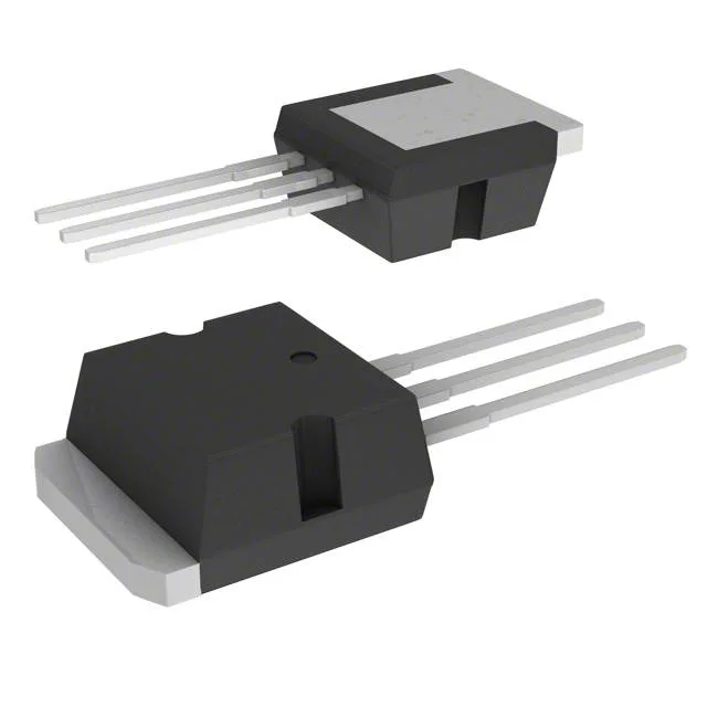
600 V N-channel MOSFET in I2PAK — offline power conversion workhorse
It is housed in a through-hole TO-262 (I2PAK) package, intended for high-voltage switching applications such as power-factor-correction stages, flyback and forward converters, and two-switch topologies in offline power supplies.
On-resistance and gate charge — switching loss trade-off
Input capacitance measures 1060 pF at 100 V drain-source bias.
Temperature range and thermal design
Maximum power dissipation is 150 W at case temperature, which demands a heatsink sized for the application's duty cycle. The through-hole I2PAK package provides a direct thermal path to the PCB or heatsink via the metal tab.