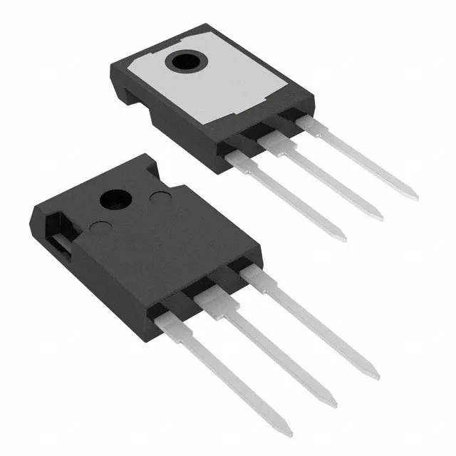
STMicroelectronics STGWA30M65DF2

STGWA30M65DF2 IGBT, 650 V, 60 A, Trench Field Stop, TO-247-3

MPNSTGWA30M65DF2
End of Life

STMicroelectronics STGWA30M65DF2, Trench Field Stop IGBT, 650 V Vces, 60 A Ic, 2 V Vce(on) typ, 80 nC Qg, TO-247-3 Long Leads, -55 to 175°C.

$3.57Ref. price · indicative, final on quote
PackagingTO-247-3
StockContact for availability
MOQ1 pcs
  • 100% new & originalTraceable channels only — no refurbs, no pulls, no remarked parts.
  • Date & lot codes on quoteStated per line before you commit; label photos on request.
  • MSL-compliant ESD packingMoisture-sealed bags with indicator cards; reels photo-verified.
  • PayPal buyer protectionPay by T/T, PayPal or Payoneer — card payments covered end to end.

Specifications

STGWA30M65DF2 Technical Specifications
ParameterValue
IGBT typeTrench Field Stop
Input typeStandard
Mounting typeThrough Hole
Voltage - collector emitter breakdown650 V
Current - collector (Ic)60 A
Current - collector pulsed120 A
Power - max258 W
Operating temperature-55°C ~ 175°C (TJ)
PackageTube
Gate charge80 nC
CaseTO-247-3
Test condition400V, 30A, 10Ohm, 15V
Switching energy300µJ (on), 960µJ (off)
Td (on/off) @ 25°C31.6ns/115ns
Vce(on) (Max) @ vge, ic2V @ 15V, 30A
Reverse recovery time140 ns

Product details

650 V, 60 A Trench Field Stop IGBT in TO-247-3

The STGWA30M65DF2 is a 650 V, 60 A Trench Field Stop IGBT from STMicroelectronics, housed in a through-hole TO-247-3 package with long leads. It targets hard-switching applications such as motor drives, uninterruptible power supplies, and power-factor-correction stages where low conduction and switching losses are required.

Conduction and switching loss at 30 A

At the test condition of 400 V, 30 A, 10 Ohm gate resistor, and 15 V gate drive, the typical Vce(on) is 2 V — this sets the conduction loss floor at 60 W for a 30 A load. The switching energy totals 1.26 mJ per cycle (300 µJ turn-on, 960 µJ turn-off), which drives the thermal design for hard-switched topologies at moderate frequencies. The 80 nC total gate charge and 31.6 ns / 115 ns turn-on/turn-off delay times (at 25°C) give the gate-driver designer the numbers needed to size the drive current and set dead-time margins. The co-packaged diode has a 140 ns reverse recovery time, relevant for inductive load clamping.

Junction temperature range and thermal budget

The 258 W maximum power dissipation assumes the case is held at 25°C; real-world derating follows the datasheet curve.

Frequently asked questions

Is STGWA30M65DF2 obsolete or discontinued?

No — the product status is listed as active.