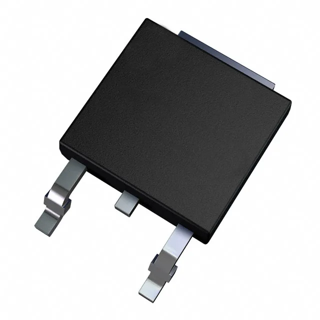
The 12 A continuous collector rating (24 A pulsed) supports 6 A test-condition switching at 400 V, 15 V gate drive through a 22-ohm gate resistor — a common hard-switching benchmark for appliance and light-industrial inverters.
Switching losses and thermal budget
Turn-on energy is 36 µJ, turn-off is 200 µJ at the 400 V, 6 A test point. The off-loss dominates the total switching loss — at 20 kHz the IGBT dissipates roughly 4.7 W from switching alone, plus conduction loss from the 2 V Vce(on) at 6 A. The 88 W max power rating leaves margin if the junction is kept under 175 °C, but the DPAK's thermal pad on a 1 oz copper pour will be the practical limiter. Gate charge is 21.2 nC — a standard 1 A gate driver charges the input capacitance in about 21 ns, which aligns with the 15 ns turn-on delay and 90 ns turn-off delay at 25 °C. The 140 ns reverse recovery time in the co-pack diode sets the dead-time floor for half-bridge legs.
Package, footprint, and traceability
DPAK (TO-252) with two leads and a tab — the tab is the collector, so the PCB copper pour under the part must be sized for the collector current and thermal dissipation. The laser etch on the top face carries the date-code and lot traceability; a clean, consistent font is the first screen for genuine ST parts in the independent channel.
Sourcing posture and lifecycle
The M series is an established ST trench-field-stop family, so PCN risk is low for the near term. If dual-sourcing is required, parametric screening against other 650 V, 12 A DPAK IGBTs with similar Vce(on) and switching energy is the practical path — pin-compatibility is not guaranteed without a layout review.